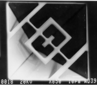
Figure (5) shows a SEM microphotograph of a balanced resonator
Presented and published
Proc. Of SPIE, volume 3903, p32-41, (1999)
Study of vibrational modes of MEMS-resonators
S.G. Lokhre, K. Virwanif , B.
Gajananf , S.P. Pai, P.R. Apte
Solid State Electronics Department
Tata Institute of Fundamental Research
Homi Bhabha Road
Colaba, BOMBAY - 400 005, India
e-mail : lokhre@tifr.res.in
or apte@tifr.res.in
Fax : +91-22-215 2110 or +91-22-215 2181
fDepartment of Mechanical Engineering
Datta Meghe College of Engineering
Airoli, New Bombay 400 708, India
ABSTRACT
We have designed, fabricated and tested a balanced doubly suspended versatile, torsion and flexural, MEMS resonator structure. The doubly suspended structure has been used earlier for very precise high Q resonators but we wished to study the various vibration modes of such a structure. FEM analysis has been used to compute the most likely 6 modes and their frequencies of free vibration. These modes include flexure, torsion and mixed modes. The arms of the resonator are deposited with magnetic films so as to give desired bending/twisting moments to the structure. The location of the films decides the symmetry and thus result in one of the six vibrational modes that are predicted by the FEM analysis. This paper describes the design, fabrication and measurements on resonator structures made at TIFR.
Keywords: micromachines, MEMS, Anisotropic etching, resonators, smart materials, actuators
1. INTRODUCTION
Traditionally silicon has been the bane of transistor and integrated circuit (IC). It paved on the way to very large scale integrated circuits (VLSI) wherein the device structures were of the order of few microns. Apart from this phenomenal success in the field of microelectronics, silicon has now provided the micro-electromechanical-systems (MEMS) wherein micron sized structures are fabricated in single crystals of silicon as mechanical sensing devices.
These microstructures made of SiO2 having dimensions 1-10 micron in width and 50-100 micron in length were suspended over a 100 micron deep cavity in silicon. The 100 micron X 100 micron square cavity was obtained by a crystallographic etchant KOH. Such microstructures then bend or vibrate in the cavity formed giving a 3D like effect to the devices. Some of the microstructures fabricated in our laboratory 1 are as follows namely Cantilevers, Cross-bridges, Spirals, Doubly suspended resonators, Micro-probes, Magnetic sensors etc. These microstructures were subjected to different treatments for different applications, like evaporation of metals for thermal applications or sputtered with magnetic materials for magnetic actuator like applications etc.
Its main advantages lie in the similar process of fabrication of sensor structures to that of VLSI devices in microelectronics. MEMS has another added advantage of providing both mechanical sensor and electrical circuits, placed side by side on a single silicon crystal, leading to reduction in number of stages involved in converting signals from one form to another and the noise thus generated. A 50 g accelerometer in single crystal silicon integrated with an ASIC signal conditioning circuit and packaged in a 16-pin plastic DIP or alternatively in an SOIC package by U. Shridhar and a team from the Microelectronics, Singapore and EG&G Heimann, Singapore has been reported in the 1998 IEEE International Electron Devices Meeting in San Francisco.
MEMS devices can be optically excited by modulated light guided by a fibre and detected by photosensitive or photothermal (direct conversion of pulsed light into mechanical vibrations is known as photoacoustic principle) devices. It can be ultrasonically excited by ultrasonic piezoelectric sources and detected by photoacoustic devices. Micromachined structures having magnetostrictive properties are very sensitive to applied magnetic fields and can be detected by magnetic field sensing devices like Hall effect devices.
Lots of MEMS devices have been fabricated to work as very precise high Q torsional oscillators 2 and magnetic sensors 3 in silicon. But here we have designed, fabricated and tested a balanced doubly suspended versatile, torsion and flexural, MEMS resonator structure to study the various vibration modes of such a microstructure. Finite Element Structure, (FEM) analysis has been used to compute the most likely 6 modes and their frequencies of free vibration. These modes include flexure, torsion and mixed modes. The arms of the resonator are deposited with magnetic film so as to give desired bending/twisting moments to the structure. The location of the film decides the symmetry or rather mars the symmetry and thus result in one of the six modes of vibration that are predicted by the FEM analysis. Design, fabrication and measurements on deliberately unbalanced resonators structures made at TIFR will be presented in this paper.
2. DESIGN
2.1. MICRO RESONATORS IN VARIOUS MODES OF VIBRATION:
To set a resonator in vibration, the micro resonator has to be deliberately made unbalanced. This is achieved by treating different portion of the resonator structure with different effects i.e. made magnetic as in our case, depending upon various modes of vibration as suggested by FEM Analysis tool used from CADRE Analytic, USA. The basic frequency of vibration is around 3 Mhz. CADRE is a finite element analysis program designed to solve static and dynamic structural frame problems. The structural model is controlled using a series of data entry form which includes defining the nodal coordinates, element properties and connections, boundary conditions, loading conditions or mass and inertial data for dynamic needs. There are two types of operations available in CADRE namely static and dynamic. The dynamic operations are used here for solving vibration modes and finding their frequencies for 4 basic modes.
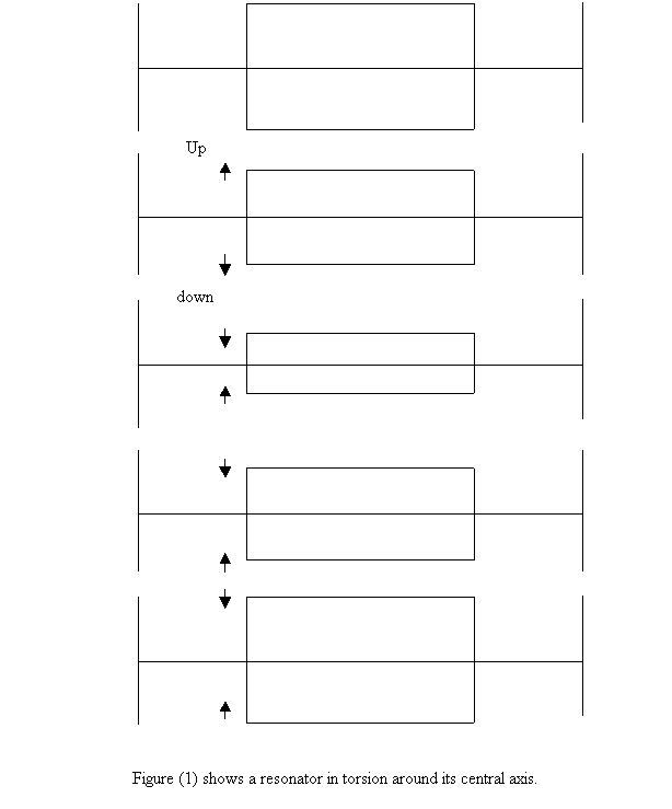
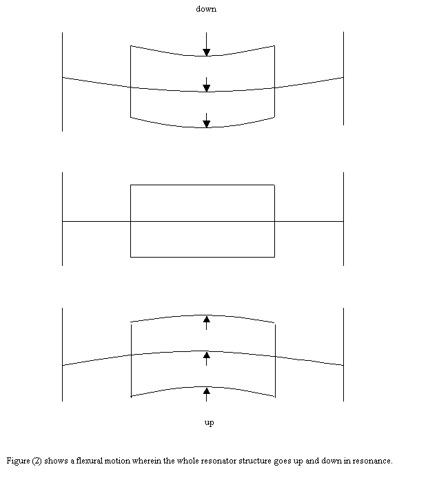
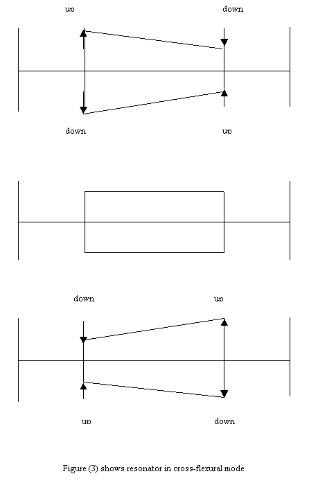
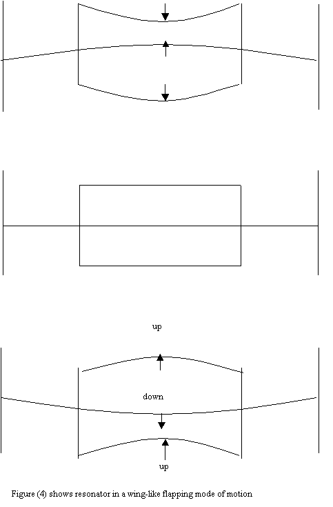
Following figures are the plots as traced from FEM results. Figure (1) shows a resonators outer arms in torsion around its central axis at 70 times the resonance frequency. Figure (2) shows resonator in a flexural motion wherein the whole resonator structure goes up and down in resonance at 88 times the basic resonance frequency. Figure (3) shows resonator in cross-flexural vibration wherein the resonator structures, one set of diagonally opposite corners go up while the other set goes down in anti-phase motion around its central plane at 240 times the basic resonance frequency. Figure (4) shows resonator in a flapping mode of motion wherein the outer arms of the resonator structure goes up when its central arm goes down at 330 times the basic resonance frequency. This motion is similar to that of a birds wing flapping or flying motion.
One arm is made positively effected to get torsional motion around the central axis. All the three namely central and both the end arms are made positively effected for the flexural mode. Diagonally opposite corners of the resonator is made positively effected to get cross-flexural motion. And both the arms are made positively effected to get birds wing like flapping mode of vibrations.
A positive effect means that portion of the resonator structure is subjected
to a special treatment whereas the rest of the resonator structure is without
it. And a negative effect means that portion of the resonator structure
is without the magnetic film and the rest of the resonator is left with
it.
2.2 PATTERN DESIGNING:
The pattern is designed by DesignCad 2D package using a 80486 IBM compatible PC. The pattern is designed in three stages. First stage consists of 12 number of balanced micro-resonator structures along-with the plus shaped alignment mark at the extreme ends. Each resonator is of 10 micron in width, 100 micron in length and placed in an area of 140 X 140 square microns. All the 12 resonator structures and the alignment marks are within an area of field 900 X 900 square micron. The magnification is around 100X. This pattern is a negative kind such that after exposure it will generate a mask of SiO2 on the surface of silicon.
The second stage consists of only two windows at the extreme ends containing the plus shaped alignment mark. The alignment marks are designed such that a resolution of about a micron is achieved to guarantee proper alignment of the patterns. Again the magnification has to be same i. e. 100X. This is called as the "Align " pattern.
And the final stage consists of the "Effects" pattern wherein only a part of the resonator structure, say only arms, is exposed. This Effects pattern consists of 12 small patterns from different part of the resonator structure as suggested by the different vibration mode using FEM Analysis tool from CADRE. Basic four types of modes namely: torsional mode, flexural vibrations, cross-flex modes and wing flapping mode would be discussed here.
3. FABRICATION
The designed pattern is transferred on a chrome plate by using the PC based electron beam lithography (EBL) attachment to JEOL JSM-840 scanning electron microscope (SEM). Only the first stage designed whole resonator pattern with the alignment marks is exposed and etched on a chrome plate coated with e-resist. This chrome plate is used as a photomask to transfer patterns on oxidised silicon substrates by conventional photolithography technique. This reduces the time taken to prepare many samples compared to the time taken for direct write using EBL technique. The mechanical properties of silicon and oxidised silicon, comparable to that of steel, are of considerable importance while fabricating such microstructures. After developing the patterns are etched in oxide using BHF solution and the photo-resist from the sample is stripped off. This is called as the oxide mask in silicon.
Later the patterned silicon sample is spin coated with e-resist again. The sample is mounted in the SEM with rough visual alignment and finely positioned by using the second stage namely the "Align" pattern in the alignment mode of the NPGS package. Only the windows containing the alignment mark is exposed to e beam and caution is taken that the middle part is not damaged.
Finally the last stage of the designed pattern called as the "Effects" pattern, which is only a part of the earlier exposed pattern, is exposed directly on the aligned sample. The sample is sputtered with cobalt (a magnetic film) and developed. Cobalt thin film remains on the exposed arm and is lifted off from all the other remaining places. This is called as "lift-off technique". The sample is then subjected to anisotropic etching of silicon in KOH a crystallographic <111> stop etchant for about 100 minutes at 80 ° C which has to be maintained constant for proper etching quality.
Figure (5) shows a SEM microphotograph of a balanced resonator after the anisotropic etching. The arms of the resonator are 5 m m and the torsion strings are 2 m m. The entire resonator is suspended on a 100 m m trapezoidal cavity.
4. MEASUREMENTS
Magnetic deflection measurements were carried out on a HALF-resonator structure by observing the deflections under an Optical microscope. The deflections were calibrated in terms of micrometer scale readings on the focussing knob. When a rare earth magnet was brought very close to the sample from underneath the resonator structures deflection was observed as a function of the displacement in mm of the magnet from the resonator. The magnet was mounted on a translational screw arrangement and the rotations were recorded. Then the same procedure was repeated by replacing the resonator sample by a Hall effect device connected to a Gaussmeter to measure the magnetic fields. This shows that the deflection is linearly dependent with the magnetic fields.
When a rare earth magnet is brought close from underneath, then the micro resonator will move in such a way that the magnetic coated arm will get attracted down first and the other arm will go up, twisting at the central arm. Then because of torsional force at the central arm which acts like a steel wire of about a micron width, tension develops and the magnetic arm gets repelled away from the magnet and the other arm goes down at the resonance frequency. This is called as resonator structure in torsion mode.
Reliability of the resonator structure is very good. The micro-resonators survived even after a period of two years and the deflections were observed after a gap of four months indicating the tensile strength of the oxidised silicon resonator structures which was only a couple of micron wide.
5. CONCLUSIONS
We have successfully designed, fabricated and tested a balanced doubly suspended versatile, torsion and flexural, MEMS resonator structure with very high Q. FEM analysis has been used to compute the most likely 4 modes and their frequencies of free vibration. These modes include flexure, torsion and mixed modes. The arms of the resonator are deposited with magnetic film so as to give desired bending/twisting moments to the structure. The location of the film destroys the symmetry and thus result in one of the four vibrational modes as predicted by the FEM analysis.
6. REFERENCES
Figure (5) shows a SEM microphotograph of a balanced resonator
Go back to MEMS page
Go back to Apte's web-page