Presented and published
Proc. of SPIE, vol. 3903, pp 223-231
A current controlled curled tip
P.R. Apte, S.G. Lokhre, S.C. Purandare, B. Gajananf , K. Virwanif
Solid State Electronics Group
Tata Institute of Fundamental Research
Homi Bhabha Road
Colaba, BOMBAY - 400 005, India
e-mail : apte@tifr.res.in
or lokhre@tifr.res.in
Fax: +91-22-215 2110 or +91-22-215 2181
f Department of Mechanical
Engineering
Datta Meghe College of Engineering
Airoli, New Bombay 400 708, India
ABSTRACT
There have been several cantilever-based actuators which provide movement in a direction transverse to the length of the cantilever. Here we describe a novel actuator which gives movement in the same direction as that of the length of the element. This is achieved by a curling up action of a bimetal like 'metal on silicon dioxide' straight element due to large differences in the coefficients of linear expansions and the high temperature which is obtained during the metal deposition.
The cantilever is made from a silicon dioxide patterned in the shape of an acute angled ">" tip which is aligned to the major flat of silicon wafer. The width at the base is 10 um and reduces to 2 um near the tip. During the cavity etching, the silicon etching starts at the tip and slowly moves under the silicon dioxide. In about 120 min etching in KOH/IsoPropanol/Water etchant at 80C, the etching under the tip moves right upto the base of the ">" shaped tip. Furthermore, advantage is taken of the fact that KOH etchant etches thermally grown silicon dioxide at the rate of about 1500 Angstrom/hour. This results in a tapered oxide tip. The tapering in width as well as in thickness help develop a higher temperature at the tip during the metal deposition by filament evaporation. On cooling, the tip bends towards the metal side due to large contraction in metal as compared to that of oxide. We routinely get U-bends and have achieved even multiturn curling.
Keywords: micromachines, MEMS, Anisotropic etching, cantilevers, current sensors, smart materials, actuators
1. INTRODUCTION
These microstructures, made of SiO2, having dimensions 1-10 micron in width and 50-100 micron in length were suspended over a cavity of 140 micron deep in <100> in silicon. The 100 micron X 100 micron cavity is obtained by a crystallographic etchant KOH. Such microstructures then bend or vibrate in the cavity formed giving a 3D like effect to the devices. Some of the microstructures fabricated in our laboratory 1 are as follows namely Cantilevers, Cross-bridges, Spirals, Doubly suspended resonators, Micro-probes, Magnetic sensors etc. These microstructures were subjected to different treatments for different applications, like evaporation of metals for thermal applications or sputtered with magnetic materials like Cobalt for magnetic actuator like applications etc.
Applications of MEMS today are very wide. But to begin with mostly simple microstructures like Cantilevers and Resonators were used. Cantilevers were used as the humble devices as Temperature sensors using the bimetallic principle. Resonators were used as the magnetic sensors.
Cantilevers, in our laboratory have been designed, so
as to be used as the first moving or bending sensor. Such cantilevers traditionally
have provided movement in a direction transverse to the length of the cantilever
arm. But here we describe a novel actuator, which gives movement in the
same direction as that of the length of the element. The cantilever is
made from a silicon dioxide patterned in the shape of an acute angled ">"
shape. Current sensitive actuators were planned as applications for such
cantilevers. This is achieved by a curling up action of a bimetal like
metal on silicon dioxide straight element due to large differences in
the coefficients of linear expansions and the high temperature which is
obtained during the metal deposition. Such bending applications can be
used to make current sensitive or temperature sensitive contacts. The cantilevers
can be bend forward or backward where it will make contact with immovable
metallized contacts. Cantilever-based Actuators can then be integrated
with associated signal conditioning electronics for a full fledged device.
1.1. ELECTRON BEAM LITHOGRAPHY
A PC based electron beam lithography (EBL) attachment to JEOL JSM-840 scanning electron microscope (SEM) is used to generate patterns of various sizes varying from submicron size all the way to few millimeters. EBL system consists of a SEM whose e-beam is controlled by external XY scan signals generated by D-A converters through a 80486 IBM compatible PC. EBL system accepts patterns generated by DesignCad 2D package. The Beam control hardware and software setup termed as Nanometer Pattern Generation System (NPGS) has been purchased from JC Nabity Systems Ltd., USA. The Beam is switched ON/OFF by an electromagnetic blanker (Beam Blanker Device, BBD) mounted in the column of SEM.
Fabrication of masks on chrome plates as well as Direct write on wafer can be done by such an EBL system. To expose a pattern, the necessary run file has to be defined, which contains detailed information about Beam current, exposure dose, magnification, centre to centre spacing and line spacing. The exposure dose is dependent on the type of e-resist used. And the magnification, centre to centre spacing and line spacing is dependent on the dimensions of the pattern design. A dose of 140 micro Coulomb per sq.cm, at highest possible accelerating voltage, 40KV, was used to minimise lateral beam spread. Beam current of 1000 pA was chosen to achieve a smooth exposed line while keeping the total exposure time in control.
The EBL writing technique was standardised2 in terms of SEM parameters like accelerating voltage and beam current, so as to get the resolution patterns namely Rose pattern, Wheel pattern and Spiral, with reducing width towards inside, exposed on silicon substrates, spin coated with 1000 Angstrom thick electron beam resist.
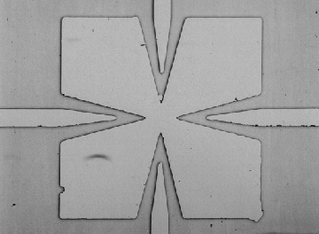
The pattern of current controlled tip is designed
using DesignCAD 2D software such that the tip is aligned to the major flat
of silicon wafer. The tip is in the shape of an acute angled ">" shape.
The width at the base is 10 um and reduces to 2 um near the tip. The length
from the base to the tip is 70 um. Four such tips are placed, one at each
side of a square of 140 um length. The base tips are extended to 250 um
length for providing a probe area in such a fashion that only four contacts
are sufficient for all the four tips. The total pattern area is about 800
um by 800 um. Hence the magnification used on SEM is 100X. The necessary
run file is then defined using the MRF command.
A photomask, generally a glass plate on which there is
a thin layer of metal, chrome is fabricated. To expose the pattern, first
the chrome plate is spin coated with e-resist and prebaked. After exposing,
the e- resist is developed, post baked and etched in chrome etchant. Now,
the chrome mask is ready for further use.
3.1. METALLISATION OF OXIDISED SILICON STRUCTURES
Evaporate Nichrome and Gold successively on the patterned wafers at slightly warmer temperatures. During evaporation a thermal stress gets created between the oxidized silicon and the metals.
3.2. MICRO MACHINING OF SILICON
This point onwards micromachining differs from microelectronics fabrication. The oxide pattern serves as a mask during "doping" of the wafer with impurities such as boron or phosphorous in IC fabrication. Anisotropic Etchants, which are also known as orientation dependent or crystallographic etchants, etch at different rates in different directions in the crystal lattice. Thus, they can form well defined shapes with sharp edges and corners. Potassium hydroxide (KOH), diluted in water is used here for the anisotropic etching of silicon. A mixture of 30 gm of KOH in 100 cc of water is used as the KOH (Crystallographic <111> stop etchant) in silicon. A mixture of ethylenediamine, pyrocatechol and water known as EDP, the organic etchant or aqueous sodium hydroxide (NaOH), a hot alkaline solution can also be used for anisotropic etching.
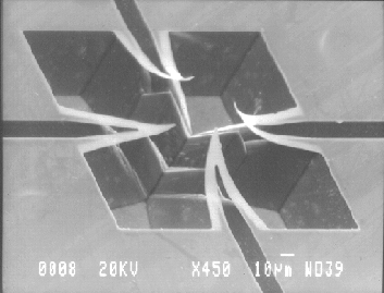
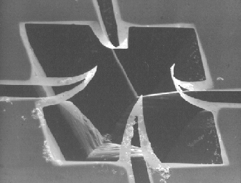
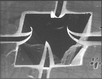
During the cavity etching, the silicon etching starts at the tip and slowly moves under the silicon dioxide structure. Cavity etching takes place at the rate of 1 micron/minute in KOH/IsoPropanol/Water etchant at 80°C. Temperature of etching should be maintained quite constant so as to get a clean etch surface, free of any muck on the side walls. The etching under the tip moves right unto the base of the ">" shaped tip. To record the change in pattern shape, wafers are etched for different times like 45 minute, 60 minute, 90 minute and 120 minute. During silicon etching tapering take place in oxide width and in thickness. This is due to the fact that KOH etchant, etches thermally grown silicon dioxide at the rate of about 1500Angstrom/hour, which is very slow compared with that of silicon, resulting in a tapered oxide tip. This helps develop a higher temperature at the tip during the metal deposition by filament evaporation leading to curl-up action. And on cooling, the tip bends towards the metal side, due to large contraction in metal as compared to that of oxide. As a result, we routinely get U-bends just like a curled up moustache! This can be observed in figure (2), figure (3), figure (4) and figure (5).
Figure (2) shows the curl-up action after 45 minutes of etching time.
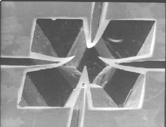
Figure (3) shows the curl-up action after 60 minutes of etching time.
Figure (4) shows the curl-up action after 90 minutes of etching time.
Figure (5) shows the curl-up action after 120 minutes of etching time.
3.3 UNCURLING OF THE TIPS
Nichrome on the oxide acts as the heating element! When current is passed through the current control tip, it gives controlled heating, which uncurls and straightens the spliced ">" tip structure tip. Such an action is seen in nature - as curled up antennae of butterflies, curled up tongues of reptiles, or curled grasp-and-hold tentacles in creepers. As we are aware that man has tried to look towards nature for mimicking various applications. We foresee applications of such current controlled ">" shaped curled tips in providing extended movements as well as in grasp-and-hold operations.
Resistance measurements were carried out on the tips thus fabricated by using a simple ohm meter on the extended gold contacts. Table 1 shows the I/V Measurements data which indicates that the resistance heater formed by Nichrome is independent of the etch duration. This data matches with the estimated resistance.4. RESULTS
Table 1 showing the I/V Measurements data.
|
|
|
|
|
|
|
|
|
|
|
|
|
|
|
Any movements in such micromachines have to be seen under microscope due to their size limitations. Uncurling of the tips was observed by flowing 1-15 mA of current through the tip using a small zoom stereo microscope because of localized heating near the tip edge. The tip fused at 22 mA of current in open air conditions due to oxidizing of the Nichrome and gold. Fusing current may increase when tip will be in vacuum or in encapsulated environment.5. RESULTS OBSERVED UNDER OPTICAL MICROSCOPE
Micron-sized current control tips were designed by Design-CAD and chrome masks made by EBL system from NPGS. We have successfully fabricated current-controlled SiO2 microtips by using micromachining technique. Curling of tip takes place due to bimetallic stresses during fabrication. And uncurling by passing control currents of the order of 1 to 15 mA. Fusing currents of 22 mA (in air) were observed.6. CONCLUSIONS
1. U.D. Vaishnav, P.R. Apte, S.G. Lokhre, V.R. Palkar and S.M. Pattalwar, "Micromechanical components with novel properties",7. REFERNCES
Proc. of SPIE, 3321, 287-297 (1996)2. S.G. Lokhre, S.C. Purandare, and B.M. Arora, " Diffraction Grating pattern on GaAs by electron beam lithography", DAE Solid
State Physics Symposium, IACS, Jadhavpur, Calcutta, Dec. 27-31, 1995
Go back to MEMS page
Go back to Apte's web-page