Figure 1. SEM micrograph of Balanced doubly suspended resonator
Micro-resonator modified as magnetic sensor
S.G. Lokhre, P.R. Apte, R.Raajeev* and R. Lal*
Solid State Electronics Group
Tata Institute of Fundamental Research
Homi Bhabha Road
Colaba, BOMBAY - 400 005, India
e-mail : apte@tifr.res.in
or lokhre@tifr.res.in
Fax : +91-22-215 2110
+91-22-215 2181
* EE Dept., IIT, Bombay-400 076, India
ABSTRACT
Balanced doubly suspended structure has been used earlier for very precise high Q resonators. But here we have used the unbalanced half section which is sputter deposited with a magnetic film. The central axis acts like a torsion wire of about a micron width and thickness. The outer arm deflects downwards about the torsion axis when subjected to a magnetic field from beneath the sample. The deflection is measured by the reflected light presently under an optical microscope but can also be done by reflecting a laser beam as done in AFMs. The bending angle -versus- magnetic field is quite linear.
To make it a smart sensor, the main suspension beams are made of 'metal over oxide' and a current flow through these gives z-movement based on the bimetallic principle.
Keywords: micromachines, MEMS, magnetic sensor, resonators, smart sensor
Micro-resonator modified as magnetic sensor
S.G. Lokhre, P.R. Apte, R.Raajeev* and R. Lal*
Solid State Electronics Group
Tata Institute of Fundamental Research
Homi Bhabha Road
Colaba, BOMBAY - 400 005, India
* EE Dept., IIT, Bombay-400 076, India
ABSTRACT
Balanced doubly suspended structure has been used earlier for very precise high Q resonators. But here we have used the unbalanced half section which is sputter deposited with a magnetic film. The central axis acts like a torsion wire of about a micron width and thickness. The outer arm deflects downwards about the torsion axis when subjected to a magnetic field from beneath the sample. The deflection is measured by the reflected light presently under an optical microscope but can also be done by reflecting a laser beam as done in AFMs. The bending angle -versus- magnetic field is quite linear.
To make it a smart sensor, the main suspension beams are made of 'metal over oxide' and a current flow through these gives z-movement based on the bimetallic principle.
Keywords: micromachines, MEMS, magnetic sensor, resonators, smart sensor,
1. INTRODUCTION
Apart from the phenomenal success in the field of microelectronics, silicon can now provide micro-electromechanical-systems (MEMS), wherein micron sized structures are fabricated in single crystal silicon 1 as mechanical sensing as well as actuating type of devices. These microstructures can have applications in diverse field like Aerospace applications, Defence applications, Biomedical applications to name a few. Structure and shape of these devices will define the type of application.
One of the many applications for such devices is in the
detection of magnetic fields. Silicon microstructures having magnetostrictive
properties are very sensitive to applied magnetic fields. They can be also
incorporated into miscroscopic areas for detection purposes like micro-hall
probes or magnetic domain measurements. Here we have used the resonator
(unbalanced half section) which is sputter deposited with a magnetic film
for magnetic sensor like applications. Design, fabrication and measurements
on deliberately unbalanced resonators structures made at TIFR will be presented
in this paper.
2. FABRICATION
2.1. Fabrication of microstructures:
The resonator pattern was designed using a DesignCAD package. Then the pattern is exposed with electron beam on a chrome plate coated with electron resist by using PC based electron beam lithography (EBL) system. EBL consists of a versatile and laboratory oriented Nanometer Pattern Generation System (NPGS) attachment to JEOL, JSM-840, scanning electron microscope (SEM). The processed chrome plate is used as a photomask to print patterns on oxidised silicon substrates by conventional photolithography technique. Typical thickness of silicon dioxide, grown in a furnace, was around 1 micron. The mechanical properties of silicon and oxidised silicon, comparable to that of steel, are of considerable importance while fabricating such microstructures. The photolithography printing technique reduces the turn around time taken to prepare many samples compared to the turn around time taken for direct write using EBL technique, as the electron resist exposure dose is normally very small. After developing the patterns on the silicon samples, silicon dioxide layer is selectively etched in buffered hydroflouric (BHF) acid mixture and the photo-resist is stripped off from the sample using Acetone. This pattern is called as the "oxide mask" in silicon 2.
After cleaning the sample, the bare silicon is etched in an anisotropic etchant. A mixture of potassium hydroxide (KOH), Isopropanol (IPA) and water serves as a crystallographic <111> stop etchant leading to a pyramidal pit with a square opening at the top. KOH etchant doesnt attack oxide layer at significant levels, leaving behind freely standing oxidised structures to move in 3D space. These are held to silicon layer at some corner and hence termed as suspended structures. These microstructures were subjected to different treatments for different applications, like evaporation of metals for thermal applications or sputtered with magnetic materials for magnetic actuator like applications etc.
2.2. Fabrication of micro-resonator:
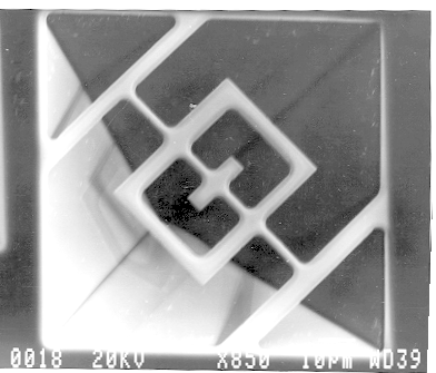
A balanced suspended versatile MEMS resonator structure
was fabricated to study the various modes of vibration. Such a balanced
resonator was suspended with an additional arm, tangentially in between
the torsion wire and the silicon structure as shown in the SEM micrograph
in figure 1. This is called as a doubly suspended resonator. This additional
arm acts as a further flexible support to the central torsion wire. This
provides a very high Q factor. The torsion wire is about few microns in
width and thickness, whereas the rest of the structure is about 10 micron
in width. The balanced resonator is suspended in a 100 micron by 100 micron
square pit formed by crystallographic etchant KOH at 80°
C for about 100 minutes.
Figure 1. SEM micrograph of Balanced doubly suspended resonator
2.3. Realisation as a magnetic sensor:
After the resonator structures are fabricated, the whole of the resonator is sputtered deposited with magnetic film (Cobalt) in a DC Sputtering system. The material and the thickness of the magnetic film has been standardised which defines the sensitivity of the magnetic sensor. The thickness of the magnetic film deposited was around 1000 angstroms such that desired bending/twisting movement can be imparted by the available permanent magnet.
But to move or deflect the balanced resonator, it had to be deliberately made unbalanced. This can be achieved by two methods either by incorporating unbalanced effect in the fabrication process or else by starting with an unbalanced pattern design. Unbalanced effect is achieved by treating different portion of the resonator structure with different effects i.e. made magnetic as in our case. This is a more complex process involving pattern alignment and lift-off techniques. Such selective "effects" can then set in different modes of vibration like flexural, torsion and their mixed modes. The location of the magnetic film decides the symmetry or rather mars the symmetry such that an imbalance is introduced.
An unbalanced pattern as entered in CAD design itself
will enable us to fabricate a Half-resonator. Because of asymmetry, the
outer arm has a preference and deflects downwards, about the torsion axis,
when subjected to a magnetic field from beneath the sample.
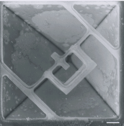
Figure 2. SEM micrograph of unbalanced half resonator
3. MEASUREMENTS
When a rare earth magnet is brought close from underneath, then the micro resonator will move in such a way that the outer arm deflects downwards about the central torsion axis. Measurements can be done either using a reflected light or a laser beam as done in an AFM system. Presently, the measurements were carried out on the resonator by observing the deflections using a reflected light under an Optical microscope as a function of the magnetic field. Varying the gap between the sample and the magnet varied magnetic field on the resonator. The deflections were calibrated in terms of micrometer scale readings on the fine focussing knob by correcting for the de-focussing observed on the outer arm. The magnet was mounted on a translational screw arrangement and the rotations were recorded.
The magnetic fields were measured by repeating the above
procedure after replacing the resonator sample by a Hall effect device
connected to a Gaussmeter. Figure 3 shows the bending angle as a function
of the magnetic field. It shows that the deflection is linearly dependent
with the magnetic fields of the order of the few KGauss.
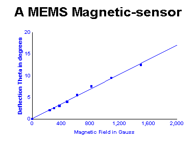
Figure 3. Deflection in degrees versus field in Gauss
4. SMART SENSOR
In order to make the sensor respond smartly, the suspended
resonator structure is metallized with gold on chrome. Thermal stress is
generated on the structure based on the bimetallic principle and it bends
upwards or downwards depending on the temperature while the metals are
deposited as shown in figure 4. Such a stressed structure will bend in
the upward direction when heated. Fig. 4(a) shows that deposition was done
at room temperature by sputtering. So on heating the gold expands more
than the oxide and hence it bends upwards as shown. The center point, where
the torsion wire of the unbalanced resonator, is connected also moves upwards.
Fig. 4(b) shows the case when gold-Chrome is deposited at 100°
C. When cooled to room temperature, the supports are bent downwards in
concave fashion. However, on heating the concavity is reduced and effectively
the center again moves upward relative to the room temperature starting
condition. Such an upward bending was observed under an optical microscope
when resonator structure was heated from room temperature of 25°
C to a temperature of the order of 60° C
in 5° C steps.
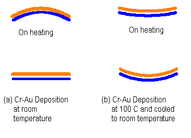
Figure 4. Shows an upward bending on heating of the bimetallic supports
Another method of bending by generating thermal stress is by passing current through the supporting arm. A device is designed such that contact pads are provided to the resonator as shown in Fig. 5. After fabrication of the unbalanced resonator in silicon dioxide, Chromium was evaporated on the resonator support arm. This chromium on the oxide acts as the heating element! Current I1 was passed through the supporting arm entering from pad1 and exiting from pad2. Due to localised heating the arm will move vertically upwards moving the resonator along with it. The center point of the support is connected to the torsion wire and this point moves up on heating. The current through the support will control the heating and hence the distance over which the torsion wire is pulled up.
Similarly current I2 was passed through
the other arm entering from pad4 and exiting from pad3
and again the resonator will move vertically upward.
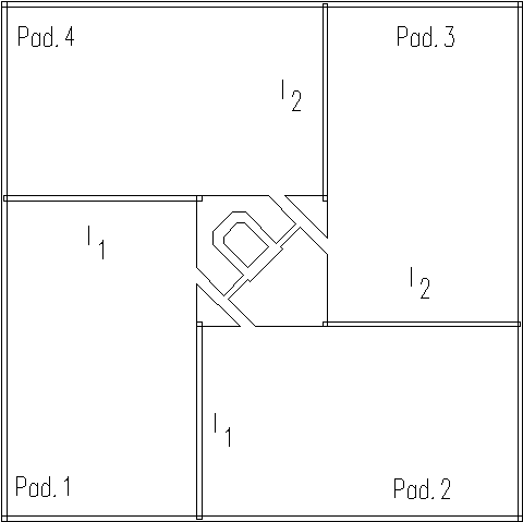
Figure 5. Shows a resonator with contact pads
5. CONCLUSIONS
We have successfully designed, fabricated and tested an unbalanced resonator. The resonator, which was sputter deposited with magnetic film, gives desired bending/twisting movements to the structure when subjected to magnetic fields quite linearly. The sensitivity of deflection depends on the magnetic material as well as on the length of the bending arm. Cobalt was used as the magnetic film. The bending arm length was maximised so that it doesnt touch the pyramidal pit throughout its deflection. The deflection was measured by the reflected light using an optical microscope.
Sensor was made to react smartly by using bimetallic principle. The suspended resonator structure is metallized with gold on chrome. Another method is to provide contact pads and flow current through the support arms. The current through the support will control the heating and hence the distance over which the torsion wire is pulled up or down.
6. REFERENCES
Go back to Apte's web-page