Abstract
Very Large Scale Integration (VLSI) of electronics components on a
silicon chip is now a mature technology. Continuing development of electronics
systems of increasing complexities in silicon and communication systems in
fiber optics has brought us to the era of Information Technology.
MicroElectroMechanical Systems (MEMS) are micrometer scale mechanical devices
that are being used in growing number of application such as communications,
computers, entertainment etc. MEMS
bring together the fabrication and manufacturing technologies of both VLSI and
precision engineering fields.
While it is
true that the precision mechanical components, micro-sensors and
micro-actuators, on their own merit justify the development effort towards
micromechanics, it should no longer be regarded in isolation from
microelectronics and microoptics. Eventually, these fields would be integrated
and emerge as a viable technology of the future.
Today, Ink-jet
printer heads and hard disk sensing heads are being mass-produced in high
volumes and hence at low costs. Texas
Instruments, USA and Sony, Japan would soon bring a variety of optical display
products that use micromechanical parts as mirrors and gratings. Micro-fluidics
is slowly catching up with medical applications like lab-on-a-chip and DNA
arrays. Importantly, the future of MEMS will be in terra-bit data storage
devices on one hand and in distributed structural control in avionics on the
other.
--------------------------------------------------------------------------------------------
This paper was presented at the
VSDT-2000 at IITB at Mumbai during 9-11 Jan 2001
--------------------------------------------------------------------------------------------
1. VLSI Technology and Moore’s Law
The 1st
Integrated Circuit was made in 1958 by Jack Kilby of Texas Instruments, Texas
USA and Robert Noyce of Fairchild
Semiconductors, California USA. The complexity of the circuits, in terms of the
number of transistors per chip, has grown at a fast pace. This was first studied by Gordon Moore and
he found that the ‘number of transistors doubled every 18 months’. This is
known as Moore’s Law. There are many aspects of this fast growth and these are
described briefly below for year 1995 – 2005,
·
component count - 1995
Pentium (5 million) per
chip - 2005 ? (1 billion)
·
critical dimensions - 1995
1 micron
- 2005 .1 micron (limit?)
·
chip size - Today centimeter
2. Silicon as a Mechanical Material
Silicon was considered as a very
fragile and brittle material and required very careful edge polishing and
handling. However, as the technology matured it was found that the whole
process could be automated using even pneumatic transport and handling at
several stages. But the real impact was only felt when Kurt E. Petersen wrote a
paper titled ‘Silicon as a mechanical material’ in Proc. IEEE (May 1982). He
stated that silicon has excellent mechanical properties which he summarised as
below,
·
Young’s modulus, Strength - ~ steel
·
no creep (perfectly elastic!) -
·
Large piezo-resistivity - converts mech to elec
Several interesting properties of silicon and IC technology were to be rediscovered for later applications,
·
Optical finish - optical
components
·
freely suspended silicon - RF components
3. micromechanical structures in sensors, actuators and systems
Some of the early devices using silicon as a mechanical material i.e.
cantilevers and diaphragms and their bending and deflections were pressure
sensors and accelerometers. Slowly more mechanical structures found interesting
effects that could lead to micro-sensors. A summary is given below,
3.1 Sensors : on freely suspended microparts
·
Piezoresistivity :– change in resistivity with stress-strain
·
Capacitive sensors :– use deflection of cantilevers/diaphragms with
respect to a fixed electrode.
·
Temperature sensor :- P-N
junction with forward or reverse bias or thermocouple voltage between hot and
cold junctions
·
Magnetic sensor :- magnetic films on cantilevers/diaphragms
·
Visible or UV or Radiation or Particle sensors :- photoconductor
or e-h pair generation
·
IR Radiation sensors :- Heat absorbed on a micro component (very low
heat capacity) results in a change in temperature which is then measured.
When mechanical structures were used for sensing, they were used in
passive mode. There was need to actuate them for getting further control on
their properties. This led to the advent of micro-actuators. A brief summary of
actuators is given below,
3.2 Actuators : to move freely suspended
microparts by generating force or torque
·
Electrostatic :– Apply potential between cantilever/diaphragm with
respect to a rigid electrode to generate a force that results in a deflection
·
Electromagnetic :– Current carrying conductor, in a magnetic field,
experiences a force that results in deflection
·
Piezoelectric :- Applied
electric potential across a piezoelectric material results in mechanical
movement
·
Magnetostrictive :- Applied magnetic field causes a change in dimension
·
Thermal :- change in temperature causes change in
dimension/area/volume or a bimetallic action results in bending and deflection
Apart from the effort to integrate sensors and actuators, a new set of possibilities opened up as more mechanical functions could be performed using available structures like, cantilevers, diaphragms, etc. More and more fully mechanical functions were realised and a summary is given below,
3.3 (mechanical)
Systems : to perform mechanical functions
·
Linear, Reciprocating or
In-plane movement in Links and mechanisms :-
A planar comb-drive on silicon provides a linear movement (using electrostatic force of attraction). This is similar to the plunger movement in a magnetic coil
·
Angular movement (restricted) :– Torsion devices, angle less
than 90 degrees
A torsion microdevice can give angular
deflection by torque generated by electrostatic or electromagnetic fields. One
end is however held firmly to the rigid silicon substrate.
·
Angular or Rotary movement (free):– Gears and motors, part or
full rotations
A comb drive can
generate linear motion that is converted to angular motion by a rack-and-pinion
arrangement. However, two comb drives, mutually at right angles, are required
to engage and disengage the rack from the pinion, so that continuous motion in
one direction can be imparted to the gears/wheels.
·
Z-axis movement :- Pivoted
mirrors with angular deflection (some part projecting outside a cavity in
silicon and other inside the cavity). Gratings made of freely suspended
sub-micron dimension digitised finger structure can be moved towards the
silicon substrate to give controlled constructive or destructive interference
of reflected light.
·
3-D movement :- Scanning in x-y plane and sensing tip movement
along z-axis
Most modern angstrom-level imaging devices like Scanning Tunnelling Microscope (STM) and Atomic Force Microscope have this requirement.
4. Synergy
between VLSI Technology and MEMS
4.1 VLSI Technology
:- A choice of compatible
materials
The VLSI technology was advanced by the time real
interest in MEMS picked up in the 80’s. A variety of materials used in VLSI were of immense importance to
the MEMS designers because these were already available in the technology. The
MEMS technology could, therefore, include these in its own processes. Many
other aspects were also useful in MEMS, these
are briefly described below,
a) Silicon
dioxide :
i)
stable mechanical properties
ii)
amorphous and isotropic
iii)
under compressive stress
b) Silicon Nitride :
i)
stable mechanical properties
ii)
amorphous and isotropic
iii)
(high temperature) ceramic
iv)
under tensile stress
c) Poly-Silicon :
i)
Thick layers 5 microns or more
ii)
Electrically conducting (as electrodes)
d) Aluminium :
i)
Electrical conductor
ii)
High optical reflectivity
4.2 VLSI Technology :- Lithography,
Deposition, Selective etching
a) Lithography :
i)
Optical/UV/Deep UV (down to .6 mm)
ii)
Electron beam (for mask making and direct wafer writing)
iii)
X-ray (down to .1 mm)
b) Deposition :
i)
Evaporation, DC or RF sputtering
ii)
Chemical Vapor Deposition (CVD)
iii)
Plating, molding etc.
c) Selective Etching :
i)
Wet chemical etching
(isotropic, large undercutting)
ii)
Dry chemical etching (anisotropic,
minimal undercutting)
(a)
Reactive ion etching (RIE)
(b)
Deep RIE for trench etching
4.3 VLSI Technology and Micromachining Technologies
:
a) Bulk micromachining :
i)
structures are ‘carved’ in silicon
ii)
silicon etched from front, back or both
iii)
microparts hinged at one or more points
b) Surface micromachining :
i)
Microstructures are deposited, patterned or molded on silicon which is
used only as a mechanical support
ii)
Free microstructures are obtained by first including
sacrificial layers and then removing them
iii)
Pattern ‘structural layers’ before removing the sacrificial layers
c) LIGA and other plating/molding methods
i)
Microstructures are plated or molded on silicon (only as a mechanical
support)
ii)
Free microstructures are obtained by first including
sacrificial layers and then removing them
iii)
structures are first patterned in very thick photoresists (~ 30 mm ) or polymers (~200 mm) exposed and developed after synchrotron radiation exposures. This
is followed by thick (nickel/copper) plating
iv)
Generally, the thickness is much larger than the width, and hence these
are called high-aspect ration structures. These deflect/bend easily in lateral
dimensions (along x- or y-axis) but are rather stiff in transverse dimension
(along z-axis).
4.4 VLSI Technology and Scaling down of critical
dimensions :
The main result of scaling down is that the
mechanical devices will become smaller and smaller as a natural consequence of
linking of MEMS technologies to VLSI technology.
Small mechanical
components imply,
a)
Less area, mass/weight
b)
Large number of mechanical components in a chip (Moore’s law!?) :
c)
Ever increasing natural frequency of vibration (natural limit of useful
operation) :
The resulting
applications will be,
i)
Miniaturised microscopes/spectroscopes
ii)
Miniaturised instruments through assembly of micro-components
iii)
Faster refresh in display applications
iv)
In a array form, it will be capable of parallel processing of acoustic
and optical signals
5. Success Stories
There are a huge number of potentially exciting and profitable applications
that are being worked on all over the world and in all leading academic and
R&D laboratories. Only a few real successes have been mentioned below.
5.1 Pressure sensors and Accelerometers :
These are micro-miniaturised devices that are already
being used in commercial applications. Pressure sensors in manufacturing
industry and accelerometers are used automobiles.
5.2 Ink-Jet Printer heads :
With availability of
precision nozzles in silicon micromachining, the first ink-jet printer head was
visualised. It based on the principle that current pulse in a small heating
resistor will instantly vaporise the ink and the resulting shock will eject a
tiny drop of ink from the nozzle. This faced slow pile up of dried ink on the
heater and thus slowly degrading the vaporising capability. The later versions,
instead, based the ink ejection on a diaphragm pump. V-grooves in silicon
provide the canals for ink to flow into a linear array of nozzles arranged much
the same as in a dot-matrix printer head of earlier era. A 3 color printer
cartridge has the 3 arrays of nozzles connected via the V-groove canals to the
color ink reservoirs. For each nozzle there is a diaphragm pump operated by
piezoelectric effect.
The ink-jet printer head is
the real success story of the MEMS device. It is estimated that ink-jet
printers alone will cross $2 billion mark in a few years!
5.3 Hard Disk heads :
Hard disks are presently
based on magnetic storage. The sensing heads have to be in close proximity to
the high-speed rotating disk. Silicon sensing heads with the excellent
tribological properties of various materials used therein allow the sensing
heads to move in proximity contact over the disk surface. This is also one of the successful
professional application of silicon MEMS device.
As the future of data
storage depends much on the progress of
MEMS based STM-like devices with Read/Write capability at
angstrom-level. Terra-bit storage devices have been predicted.
5.4 Digital Micro-mirror Devices (DMD) and Digital
Light Processing (DLP)
(by Texas Instruments) :
Texas Instruments have
already announced a digital light processing chip that will revolutionise the
image projection systems as used in TV and cinema. It is based on MEMS pivoted
mirrors at 1000 X 1000 pixel locations. The mirrors are tilted by electrostatic
signals and the strong laser light beam that illuminates the DLP chip then
reflects the light to the specified pixel location on the screen or is
reflected away from screen (into a black area). The fig.1. shows the exploded view of the micromirror assembly in
the DLP chip.

Figure 1 An exploded view of the micromirror assembly
in the DLP chip (taken from Texas Instrument web-site)
5.5 Grating Light Valve (by Silicon Light Machines)
:
Silicon Light Machines have
found a novel use for a optical grating made in silicon nitride. Instead of using the grating for selecting
the wave length of an incident light beam (by Bragg diffraction), the alternate
nitride grating fingers were pulled down by
l/4 (by using electrostatic potential) thus
giving a destructive interference and thus acting like a ‘light valve’ –
turning light ‘on’ and ‘off’.
For potentials that deflect
partially, the interference is partial and thus the chip is capable of ‘grey’
levels – fully bright to fully dark.
With ‘grating light valves’ at each pixel position and illuminating it
by a laser with appropriate lens, an image can be projected on a screen. Thus
the GLV’s have the potential of replacing monitors and TV screens in near
future. The fig.2. shows a simplified picture of the GLV (taken from the
Silicon Light Machines’ web site).
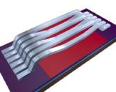
Figure 2 A 'Grating Light Valve' (from the web-site
of Silicon Light Machines)
6. SCOPE
and FUTURE
The present scenario of MEMS is warming up to a variety of immediate
and future applications. However, it is not possible say anything definite
about whether the applications fall under the current scope of activities or
lies far in the future!
A brief discussion on various possibilities for MEMS applications is
given below,
6.1 Existing MEMS - Pressure sensors and
Accelerometers :
Two prominent MEMS devices are already in the
market. The pressure sensors and the accelerometers have already been entered
volume production and have thus increased their market share.
6.2 Military Applications :
Today, most of the military applications use a few
sensors that are made smart by electronics. In future, guidance systems will
have many smart sensors with collective intelligence.
6.3
Optical Switches :
Fiber optics communication can use many of the MEMS
devices for switching light from one fiber to another. The cellular technology
can also use MEMS Radio Frequency devices in switching applications. In future,
MEMS based variable gratings would find use in selecting wavelengths in the
‘wavelength multiplexing’ systems in fiber optics communication.
6.4
Optical Benches and Optical Aligners :
Today, silicon is used as a micro-optic bench for aligning
various components like laser diodes, micro-mirrors, micro-lenses, fibers etc.
This makes the systems compact, mass producible and lower costs. In future,
silicon will provide the basic guiding rails for fibers and mounting locations
for other optics devices that are individually made smart – sense, actuation
and control functions are integrated.
6.5 Parts handling in manufacturing (robotics)
:
In today’s robots, microsensors sense dimensions,
orientations and sort into separate bins. In future, micro-robots will
recognise pattern and shapes, will pick up and correct orientation and guide
parts through obstacles etc.
6.6 Pumps, Valves
and micro-fluidics (pneumatics and hydraulics applications)
Today, Ink-jet printer head is the big success of
the micro-pumps combined with precision micro-nozzles. In near future, we
expect drug delivery systems consisting of smart micro-sensors and
micro-actuators to be implanted near an organ. Recent developments in
‘lab-on-a-chip’, microarrays and DNA chips have ushered us into an era where
medicine will be tailor-made for an individual for maximising its effectiveness
at a very affordable price.
6.7 Inertial navigation and other space
applications:
Today, the 3-axis accelerometer or gyroscope forms
the basic measuring component and the control/actuation of thrusters is
performed by electronics and computers. In future, micro-satellites, that are
just a few kilograms in weight, will have MEMS based devices for gyroscopes and
micro-thrusters.
A UC Berkeley project aims at spraying micro-sensors
(called ‘micro-dust’) in atmosphere. The ‘micro-dust’ will collect and send
environmental data by telemetry to base station. This may be vital before
entering a ‘hostile’ or ‘chemically hazardous’ zone. It may have many civil or
military applications.
6.8
Terra-bit data storage :
Today’s data storage is based mostly on effects that
are magnetic, optic or combination of the two. These require a disk to rotate
at high speeds with a sensing head in close proximity to the rotating surface.
The future data storage envisages a scanning type device based on MEMS
technology with ‘no rotating parts’. An
array of Micron sized beams, carrying Scanning Tunnelling Microscope (STM) tips
will scan over a centimetre area and can store over terra-bit data.
6.9
Structural control in avionics :
Today, prototype wings are being made with thousands
of cantilevers and air-eddy sensors. The wind tunnel tests have indicated that
the cantilevers, when raised perpendicular to the surface, give similar results
as those given by large moving surfaces on a wing – like the flaps, slats and
ailerons. This demonstrates that in future the ‘smart skin’ wings will allow
quicker turning, stabilization against turbulence and better fuel efficiency by
reducing the drag on the wing.
7. DISCUSSION
The MEMS technology has evolved from the initial start as a subset of the VLSI technology. It maximised the advantages of using the basic processes from the IC technology that were meant for microelectronics devices. Naturally, very good physical sensors were made in silicon. With more mechanical structures becoming available after the advent of surface micromachining, the MEMS technology has now pushed ahead on its own. However, the ideal goal of integrating both micromechanical as well as microelectronics components on the same chip keeps these two technologies together.
8.
REFERENCES
[1] Kurt E.
Petersen, “Silicon as a mechanical material”, Proc. IEEE, Vol. 70, No.5,
May 1982, pp. 420-457,
[2] James B. Angell, Stephen B.
Terry and Phillip W. Barth, “Silicon Micromechanical Devices”, Sci. Am., Vol. 248, No. 4, 1983, pp.
36-47,
[3] Gary Stix, “Trends in micromechanics :
Micron Machinations”, Sci. Am., 1992. pp. 107-117
[4] K.J. Gabriel, “Engineering
microscopic machines”, Sci. Am., 1995, pp. 118-121,
[5] web-site of
Texas Instrument for DMD and DLP chip, http://www.dlp.com/
[6] web-site of
Silicon Light machines for GLV technology, http://www.siliconlight.com/