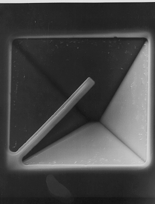
Fig. 1. Cantilever
Permission was sought and given for use in the following book
"Electronic materials and devices", D. K. Ferry & J. P. Bird, Academic
Press, San Diego (2001)
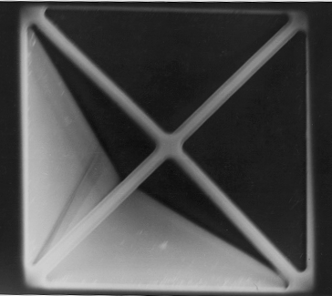
Fig. 2. Cross-beam
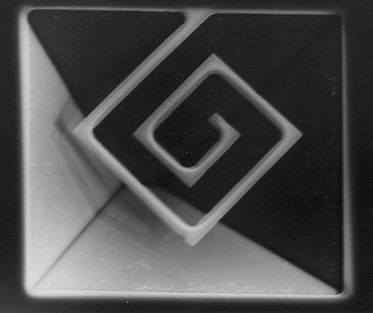
Fig 3. Spiral
Go back to MEMS-page
Go back to Apte's
web-page
A Portfolio of SEM microphotographs
of
various MEMS devices
made during
1995-2000
P.R. Apte apte@tifr.res.in
S.G. Lokhre lokhre@tifr.res.in
R. Pinto rpinto@tifr.res.in
Fax: +91-22-215 2110
Phone: +91-22-215 2971 ext. 2314
Tata Institute of Fundamental Research
Solid State Electronics Group
Department of Condensed Matter Physics
Homi Bhabha Road, Colaba, Mumbai - 400 005
India
Filename: E:\portfolio\portfolio4.doc
Date: 15-May-2000
We use Electron Beam Lithography (EBL) setup to obtain micron sized
minimum feature masks and patterns for fabricating silicon micromechanical
parts having dimensions of 1 um to 10mm. The microparts are made of silicon
dioxide, silicon nitride, P+ doped silicon, and other novel and compatible
materials (0.2 to 1um thick). These are suspended over a pyramidal cavity
obtained by a crystallographic <111>-stop silicon etchants like KOH+Isopropanol+Water
(KOH etchant) and Ethylene Diamine Pyrocatechol etchants (EDP etchant).
Specific devices and corresponding applications are as listed below,
Fig. 1. Cantilever
Permission was sought and given for use in the following book
"Electronic materials and devices", D. K. Ferry & J. P. Bird, Academic
Press, San Diego (2001)
Fig. 2. Cross-beam
Fig 3. Spiral
We made our first sensor using the unbalanced resonator structure. The
unbalanced structure made it possible to create a torque, which acts on
the torsion wire to produce angular deflection. The torque arm was deposited
with Cobalt and magnetic field was applied from below. The deflection characteristics
were measured by slowly increasing the magnetic field and using a calibrated
probe to measure this field and using microscope to measure the deflection
of the torque-arm on our device. The fig. 5a shows the SEM micrograph of
the device and Fig. 5b shows the measured device characteristics. The linearity
is excellent.
A paper titled "micro-resonator modified as magnetic sensor"
has been accepted for presentation at the SPIE-2000 symposium on "micromachining
and microfabrication" to be held at Santa Clara, CA during 18-21 Sept 2000.
10 micron bar
Fig. 5a. An unbalanced torsion resonator with cobalt (magnetic)
film
deposited on the deflecting arm
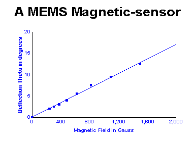
Fig. 5b. Deflection characteristics for an unbalanced torsion magnetic sensor
Current Controlled Curled Tips : (1998-99)
Cantilevers are normally used either in bending or vibrating mode. Cantilevers traditionally have provided movement in a direction transverse to the length of the cantilever arm. But here we describe a novel actuator, which gives movement in the same direction as that of the length of the element. The cantilever is made from a silicon dioxide patterned in the shape of an acute angled ">" shape. Current sensitive actuators were planned as applications for such cantilevers. This is achieved by a curling up action of a bimetal like metal on silicon dioxide straight element due to large differences in the coefficients of linear expansions and the high temperature which is obtained during the metal deposition. Such bending applications can be used to make current sensitive or temperature sensitive contacts. The cantilevers can be bend forward or backward where it will make contact with immovable metallized contacts. Cantilever-based actuators can then be integrated with associated signal conditioning electronics for a full-fledged device.
Micron-sized current control tips were designed by Design-CAD and chrome masks made by EBL system from NPGS. We have successfully fabricated current-controlled SiO2 microtips by using micromachining technique. Curling of tip takes place due to bimetallic stresses during fabrication. Etching the cavities for progressively more time give larger bending effects as seen in fig.6 (for 45, 60, 90 and 120 min etching). Uncurling is obtained by passing control currents of the order of 1 to 15 mA. Fusing currents of 22 mA (in air) were observed.
- - - - - - - - - - - - - - - - - - - - - - - - - - - - - - - - - - - - - - - - - - - - - - - - - - - - - - - - - - - - - - - - - - - - - - - - - -
Already appeared in the
Proc. Of SPIE, "Indo-Russian Workshop on Micromechanical Systems"
volume 3903, p223-230, (1999)
- - - - - - - - - - - - - -- - - - - - - - - - - - - - - - - -
- - - - - - - - - - - - - - - - - - - - - - - - - - - - - - - - - - - -
- - - - - -
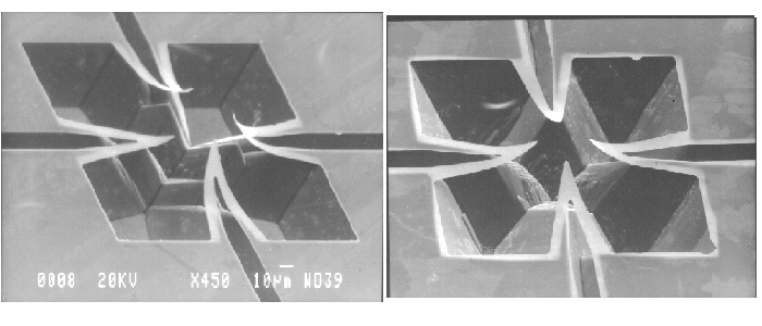
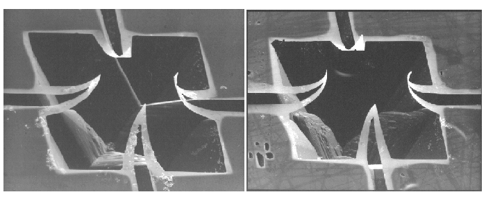
Fig. 6. Curled tips
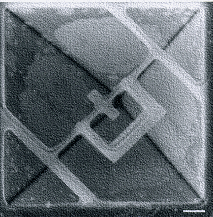
AutoRanging Torsion Sensors : (1999-2000)
Autoranging torsion sensors were conceived as a result of a conscious effort to make the sensor 'do things by itself' (this is a very important innovative concept in TRIZ - A Russian acronym for Theory of Inventive Problem Solving). We designed and fabricated unbalanced torsion (angular deflection) devices (shown in Fig. 7) that have
(3) both 1st and 2nd STOPs
(4) no STOPs but the torque-arm itself having a STOP action
The lengths of 1st STOP, 2nd STOP, torque-arm
and width of torsion wire affect the angular deflection and the linearity
of the characteristics. We have taken each of these dimensions of 3 values
- smaller, nominal and larger. The numbers of possible (factorial) combinations
are 3X3X3X3 = 81. Taguchi method uses orthogonal array (called L-9 array)
for 9 experiments for determining the best-of-81 experiments. The L-9 array
experiment has been laid down on the mask and fig. 8 shows the SEM micrograph
of the same. (device #8 is broken). Results are still to be published.
Tunnel-Tips : (1999-2000)
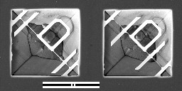
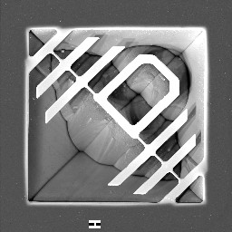
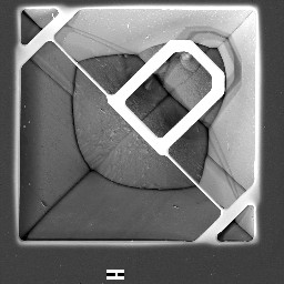
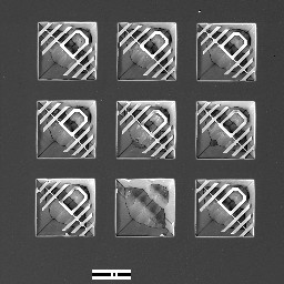
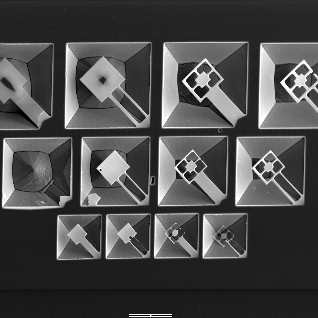
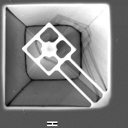
Our most recent activity is "Tunnel-tips". The objective is to obtain a 'pyramidal tip' of silicon that is pointing up and is very close to a metal pad that covers it from top. Normally, the metal pad is used for etching a tip below it and is 'sacrificed' when the tip actually gets formed (the pad has no supports and hence falls off). We attempt here to design a pad in such a way that it allows tip to be etched but does not fall off. We have more or less succeeded in this effort, as shown in Fig. 9, 10 and 11.
Fig. 9 shows various cross-bridge patterns for metal pads (and tips
forming below these after a particular time of etching. Fig. 10 shows cantilever
type patterns for pads. Fig. 10 middle-left device (with broken pad) shows
a very good quality silicon tip. Fig. 11 shows a close-up view of a single
device that has the tip just being formed below the pad. Such a device
can be used for measuring the tunneling currents. The work is yet to be
published.
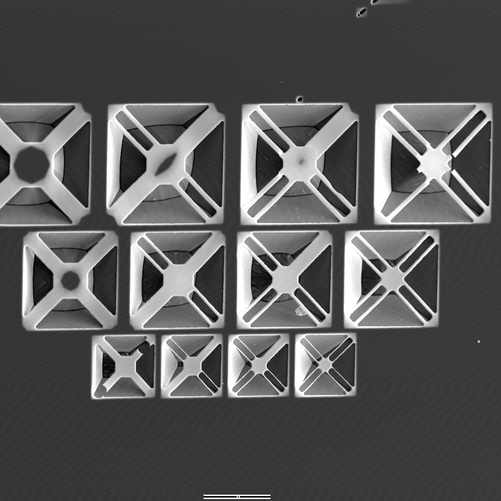
Fig. 9. Tunnel tips (cross-bridge type, various sizes, shapes)
100 micron bar
Fig. 10. Tunnel tips (Cantilever type, various sizes, and shapes)
10 micron bar
Fig. 11. A close-up of Tunnel tip (Cantilever type)
END-OF-PORTFOLIO
Go back to MEMS-page
Go back to Apte's
web-page