My main focus of research has been the improvement of power quality using power electronics. The areas are:
- Compensation in distribution systems (2003-2005)
Published a paper in the Electric Power Systems Research (an international journal listed in Science Direct) titled "Inverter topologies for DSTATCOM applications - a simulation study" that has been cited eight times to this date (refer item 1 in the Journal Publications list). Also published three papers in conferences (refer to items 4, 5 and 6 in the list of conference publications).
- Grid Connected Distributed Generators (2005-2006)
Published two papers in conferences (refer to item 2 and 3 in the list of conference publications).
- Autonomous microgrids (2006-)
Published a paper in a national conference (refer to item 1 in the list of conference publications).
In general my research interests are:
- Power Electronic Converters
- Optimal multivariable control, decentralized control, design of control for improper systems
- Embedded systems, Digital Signal Processors (DSP), real-time control
- Simulation of non-linear power electronic circuits using object oriented programming concepts in C++ and Python
- Open source software such as Linux, Real-Time Operating Systems (RTOS)
|
Below I have listed photographs of my experimental setup with a short description of each photograph. The complete experimental setup is a microgrid of three ring connected inverters.
- Inverter and associated filter
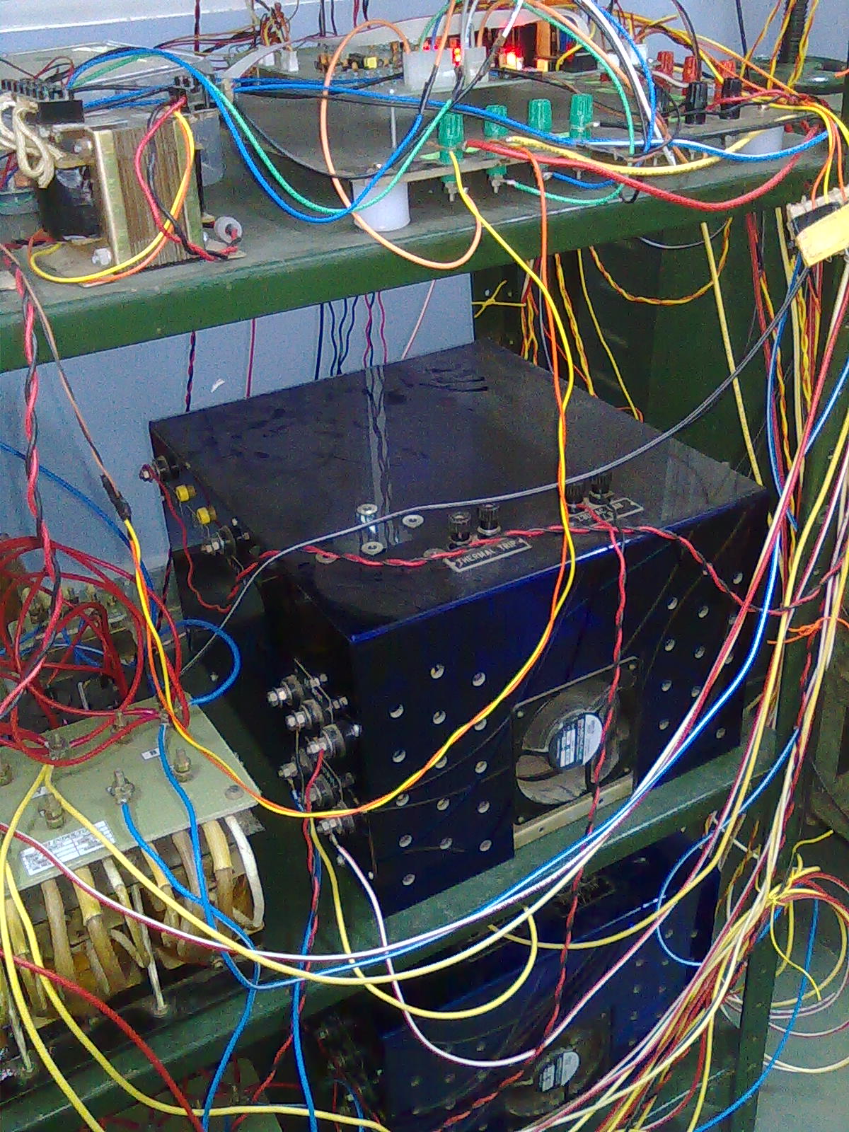
The photographs above shows the three phase inverter (blue box) with the L-C filter adjacent to it. The inverter is a six IGBT single dc capacitor three phase inverter commercially supplied by SEMIKRON. The L-C filter consists of a 3 milli henry three phase inductor with all three coils wound on the same core. The capacitor is a 200 micro farad capacitor formed by connecting four 50 micro farad capacitors (EPCOS, 440V ac). The last set of three inductors at the back are the output inductors of an inverter unit.
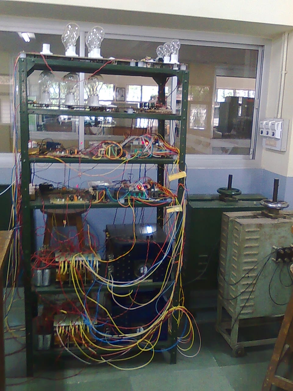
- Inverter 1
The photograph above shows the three phase inverter (blue box) with the L-C filter adjacent to it. A lamp load is seen below to form a basic resistive local load. The uppermost shelf of the rack contains the DSP processor and the sensing circuit which will described in greater detail below.
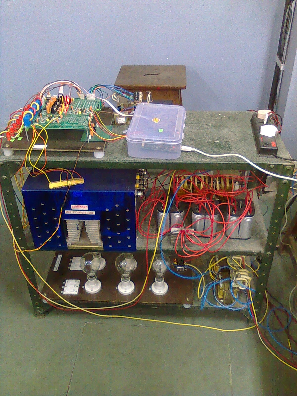
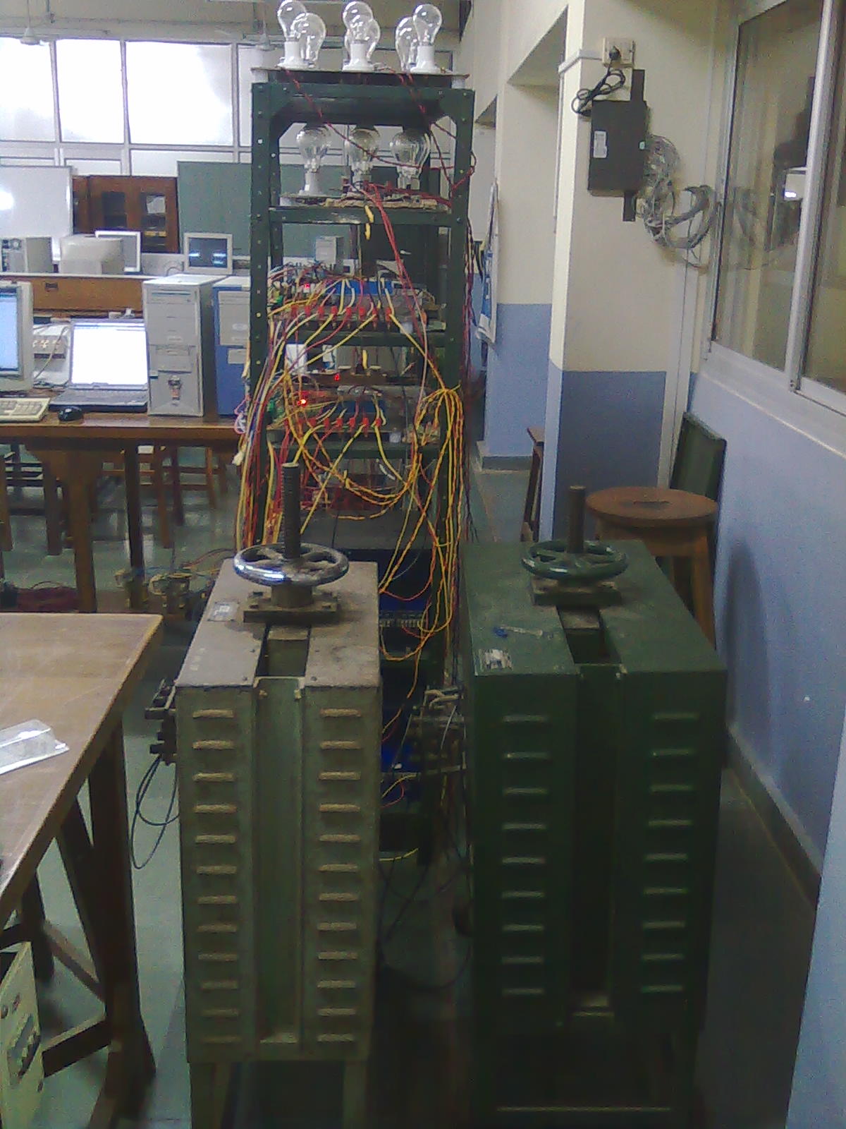
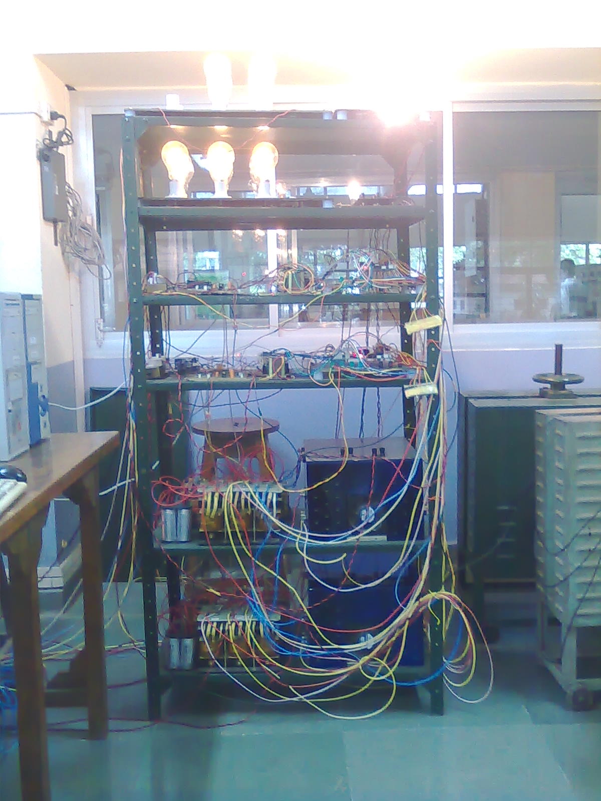
- Inverter 2 and Inverter 3
The photograph above shows Inverter 2 and Inverter 3 with their associated filter circuits and local loads. Describing the setup from bottom upwards - the first rack (lowest rack) has inverter 2 with its associated L-C filter circuits, the second rack has inverter 3 with its associated L-C filter circuits, the third rack has the sensing board, DSP board and synchronizing circuit for inverter 2, the fourth rack has the sensing board, DSP board and synchronizing circuit for inverter 3, the fifth rack has the local load for inverter 3, the sixth rack (highest rack) has the local load for inverter 3. The local load of inverter 2 has a basic three phase lamp load and also a delta connected diode bridge rectifier with output lamp load. The local load of inverter 3 has only a basic three phase lamp load
Seen on the right of the rack are two tunable reactors that are used as load that draw reactive power.
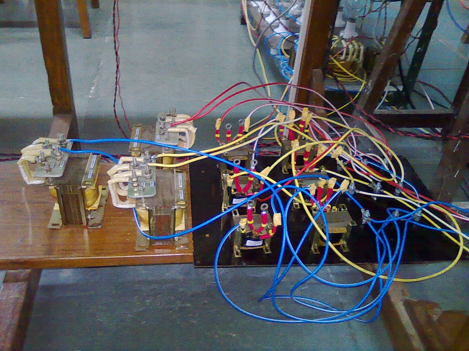
- Interconnecting Inductors
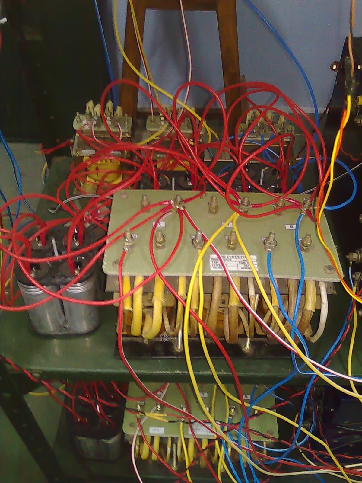
In the microgrid, the three inverters will be connected together through cables. The photograph shows the inductors that are used as interconnecting inductors since in the experimental setup, the inverters are kept close to each other. The inductors are of values between 150 - 200 micro henry.
- Isolating Transformers
In a practical microgrid, the dc bus of the inverters will be charged by sources such as photovoltaic panels, fuel cells, wind turbine driven generators etc. In this setup, the dc buses are charged by rectifying single phase ac voltages through single phase bridge rectifiers. Since, a single ac supply is available, isolating transformers are used for the three inverters to prevent a short circuit of the ac supply.
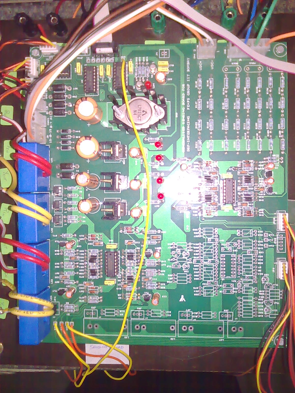
- Sensing Circuit
The photograph shows the sensing circuit used for each of the three inverters. Currents are measured using LEM current sensors (4 blue colored LEM sensors on the left of the PCB). Two sets of voltages can be measured using this sensing board. The three phase ac voltages are directly broken down using a resistor bridge network and fed to an operational amplifier (OPAMP) circuit (seen on the top-right of the PCB). The dc bus voltage of the inverter is also broken down in a similar manner using a resistor bridge network and fed to an OPAMP circuit. As the Analog to Digital Converter (ADC) of DSP board has a unipolar input range of 0 to 5V, the final output of the OPAMP circuits is a signal restricted to 0 to 5V and with a 2.5V mean.
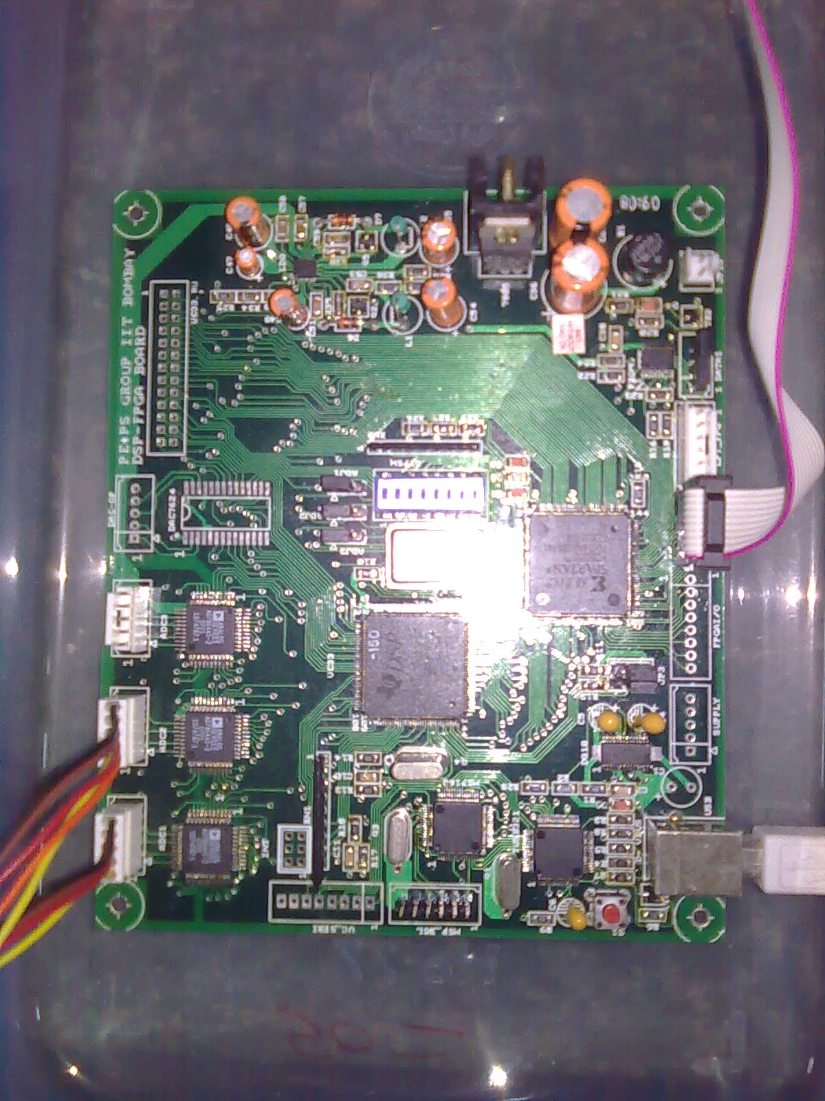
- DSP processor PCB
The photograph shows the DSP processor that executes the control algorithms. The processor used has been the floating point TMS320VC33 from Texas Instruments. The DSP processor can be seen to be roughly in the center of the PCB. To the right of the DSP processor is an FPGA - XCS3200 from Xilinx. The FPGA performs the sine triangle pulse width modulation and produces the switching signals. The switching signals and fed back to the sensing board and fed to the inverter gate drivers through level shifting ICs.
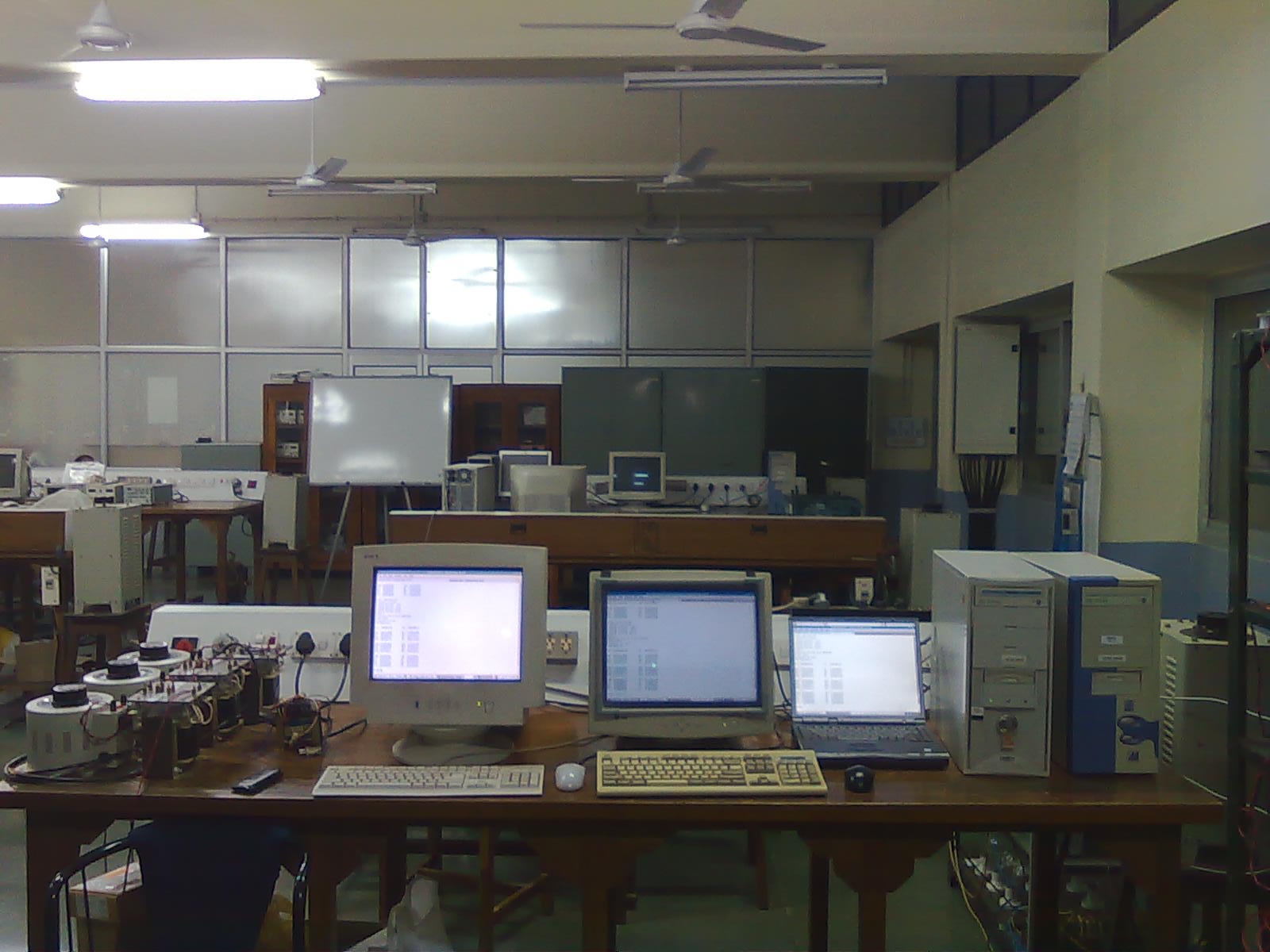
- Computers
The DSP processors run control algorithms that are downloaded onto them through computers. Only one computer can access a DSP and download the code. A provision can be made on the DSP boards to have a flash memory that will store the code and begin execution upon startup. However, in this setup, the DSP processors also behave as data loggers. Therefore, the computer can retrieve data from the RAM of the DSP processor and generate plots. The two desktop computers and the third laptop computer serve this purpose.
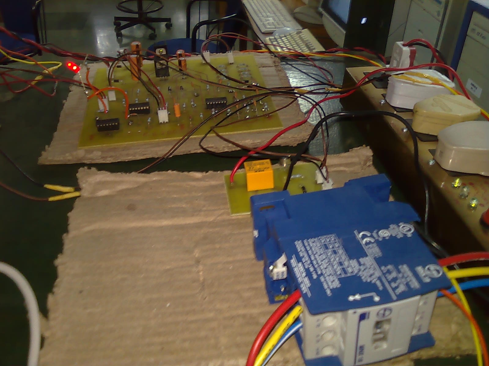
- Synchronizing circuit
The photograph shows the synchronizing circuit that connects an inverter to a microgrid to minimize transient. At the front of the photograph is the ac three phase contactor that is controlled by a 230V ac coil. Behind the ac contactor can be seen a dc relay (bright yellow colored component) that controls the ac contactor. At the back of the circuit, is the synchronizing circuit soldered on a PCB. The synchronizing circuit is an OPAMP circuit.
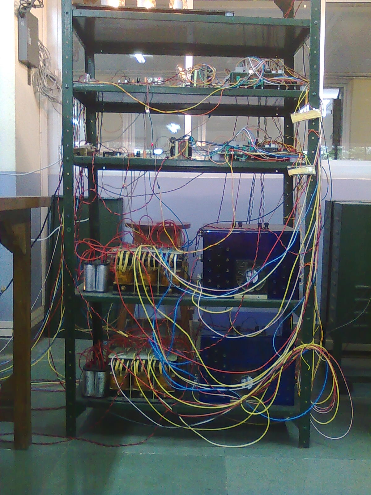
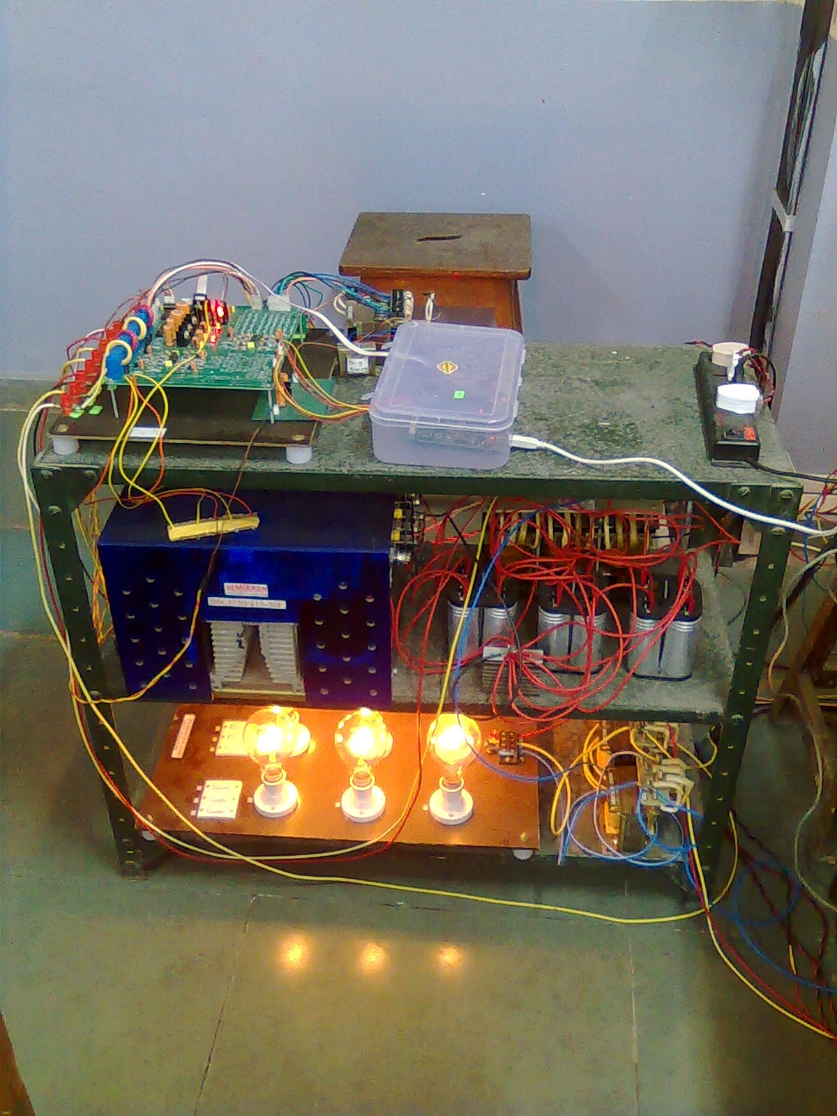
- Hardware while experiments are working
The photographs shows the hardware while experiments were being conducted. The three inverters have been connected in parallel to form a ring connected microgrid. The glowing lamp loads draw active power. Reactors can be seen to the right of Inverter 2 and Inverter 3 which draw lagging VAR. The inverters are controlled using the P-f and Q-V droops and therefore is a decentralized control without any communication between the inverters.
|