AVR
Experiment – 2
Problem Statement
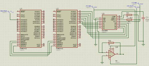
Write a program to sample sine wave signal using Internal ADC of ATMEGA 32 microcontroller (Master mode). Transmit these samples continuously to another ATMEGA 32 microcontroller
(Slave mode) using SPI communication. Reconstruct original signal from received samples using DAC0808.
Part-1
Configure Internal ADC of microcontroller. Give 100 Hz Sine wave signal to ADC0 pin. Reconstruct original signal from samples using DAC0808. Show your output to TA.
Part-2
Configure SPI and ADC peripherals of Master controller. Transmit samples continuously to another microcontroller which is configured as Slave. Reconstruct original signal from received samples using DAC0808. Show your output to TA.
Block Diagram
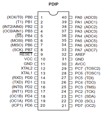
Pinout ATmega32
Typical Application using DAC0808

Sample Program
Program for Master ATMEGA32
#include<avr/io.h>
#include<util/delay.h>
#include <avr/interrupt.h>
void Port_MasterInit(void)
{
DDRA = 0xXX; // Declare direction of ADC0 pin
PORTA = 0xXX; // Declare ADC0 pin as a input.
DDRC = 0xXX; // Use port C to test output of ADC (for Part-1)
PORTC = 0xXX;
}
void ADC_MasterInit(void)
{
Configure
Internal ADC of microcontroller.
// Disable ADC, Don’t start conversion, Select prescalar value 128.
// Initialise SFIOR.
// Select AVCC (5 volts) with external capacitor at AREF pin, Adjust left.
// Enable ADC.
}
void SPI_MasterInit(void)
{
Configure SPI peripheral.
// Set direction & value of SS, MOSI and SCK pins.
// Enable SPI, Master, sample at trailing edge, set SCK rate fck/4
// Initialise SPSR
}
void SPI_MasterTransmit(unsigned char Data)
{
Write
code to transmit data.
// Make SS pin low.
// Start transmission.
// Wait for transmission to complete.
// Make SS pin high.
}
int main (void)
{
//cli () à Disable all Interrupts.
// Call functions
//sei() à Enable all Interrupts.
While(1)
{
// Start A2D Conversion.
// Wait for ADC conversion to complete.
// Transmit data using SPI communication.
// Clear ADIF flag.
}
}
Program for Slave ATMEGA32
#include<avr/io.h>
#include<util/delay.h>
#include <avr/interrupt.h>
void Port_SlaveInit(void)
{
// Use port A to send data to DAC.
}
void SPI_SlaveInit(void)
{
// configure SPI peripheral.
}
unsigned char SPI_SlaveReceive(void)
{
// Write code to receive data.
}
int main (void)
{
// Call Functions
}
Peripheral
Interface (SPI)
The Serial Peripheral Interface (SPI)
allows high-speed synchronous data transfer between the
ATmega32
and peripheral devices /other AVR devices.
Master Mode
Slave Mode
SPI Pins
MOSI
- Master Out
Slave In
SCK
– Clock Signal
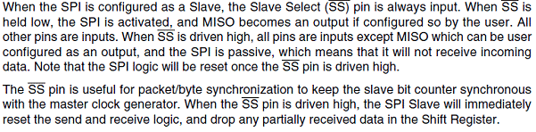
SS - Slave Select (Active Low)
MISO
– Do not use this pin.
In Master
mode define MOSI, SCK,
SS as output and in Slave mode define MOSI, SCK, SS as
input.
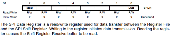
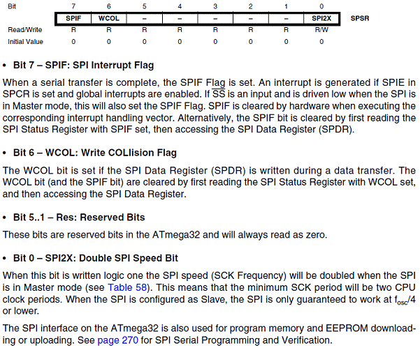
SPI Data Register
– SPDR
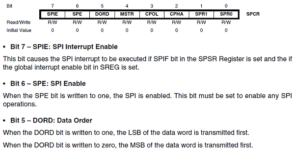
SPI Control
Register – SPCR

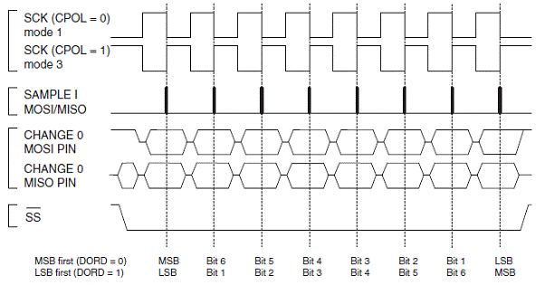
SPI
Transfer Format with CPHA = 1
SPI Status
Register –SPSR
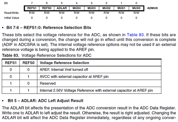
Analog to
Digital Converter (ADC)
The ATmega32 features a 10-bit
successive approximation ADC. The ADC is connected to an
8-channel Analog
Multiplexer which allows 8 single-ended voltage inputs constructed from the
pins of Port A. The single-ended
voltage inputs refer to 0V (GND). The ADC converts an analog
input voltage to a 10-bit digital value through successive approximation. The
minimum value represents GND and the maximum value represents the voltage on
the AREF pin minus 1 LSB. Optionally, AVCC or an internal 2.56V reference
voltage may be connected to the AREF pin by writing to the REFSn
bits in the ADMUX Register. The internal voltage reference may thus be
decoupled by an external capacitor at the AREF pin to improve noise immunity. Use
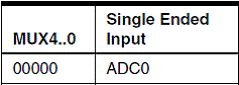
ADC0 channel for your experiment. For single ended conversion, the result is as
follows.
ADC
Output = (Vin x 256) /
Vref
ADC Multiplexer
Selection Register – ADMUX
![]()
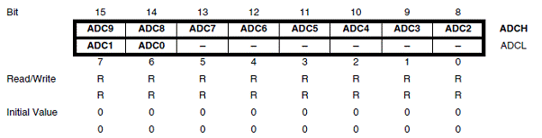
The ADC Data
Register – ADCL and ADCH when ADLAR = 1
ADC9:0 bits represent the result from
the conversion. When an ADC conversion is complete, the result is found in
these two registers. Since we are using 8 bit DAC to reconstruct signal from
samples therefore consider only ADCH byte. Neglect ADCL Byte.
Special Function
I/O Register – SFIOR
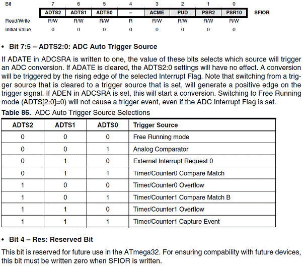
Note - Write zeros in bit 4 to bit 0
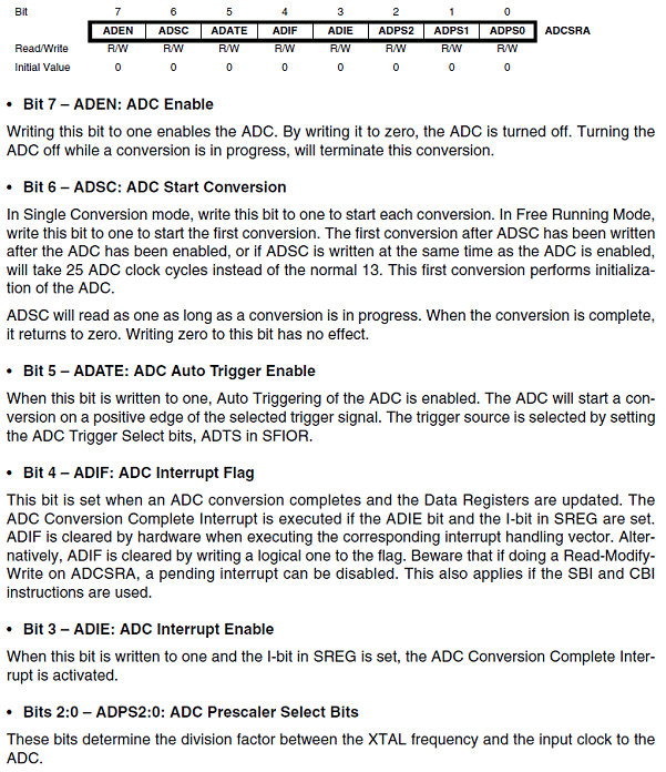
ADC Control and
Status Register A – ADCSRA

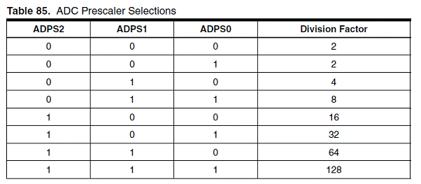
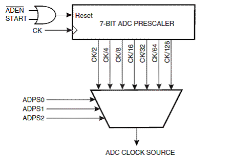
Prescaling and
Conversion Timing