H/W 3: Interfacing DAC and ADC through a
Introduction:
We
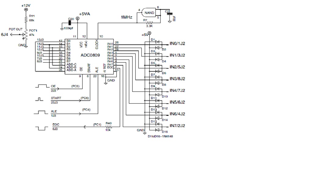
will use the ADC 0809 and the DAC 0808 for this experiment. Study the data
sheets of these components. The 0809 is an 8 bit, successive approximation ADC
with microprocessor compatible interface signals (control and data output). The
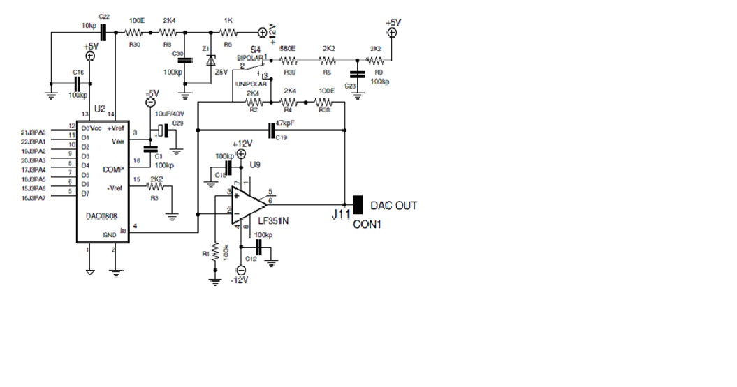
0808 is an 8-bit DAC. The circuit diagram in use for the DAC and the ADC is
also provided as part of this handout. The parallel ports of 8255 are operating
in Mode 0. You should use the BSR mode for single bit output control signals.
Problems:
1.
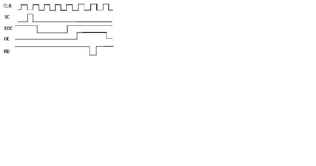
Study the data sheet of the ADC 0809 and
know the following: the timing diagram for the conversion, the width of the
"Start Conversion" signal and the conversion delay. Also, study the
circuit of ADC unit that will be used with this experiment.
2.
Likewise, study the data sheet of the DAC
0808 and know the following: the concept of a Vref, the timing diagram for the
conversion process and the conversion delay. Also, study the circuit of DAC
unit that will be used with this experiment.
3. The ADC/DAC unit (AD/DA 2) should be connected to 8255 of Classik 85 kit using 26 FRC and 4 pin relimate power connector (+/- 12V). This unit uses DAC 0808 and ADC 0809. Study the circuit diagrams for various connections.
DAC inputs are connected to Port A of 8255. The DAC output is available on tag J11. DAC current output is converted to voltage by LF 351. Switch S4 selects Unipolar or Bipolar output modes.
8 input
channels of ADC are available on 9 pin Relimate connector (J2). Channel 0 - pin
1 of J2 is connected to potentiometer (POT 1) permanently. The DC voltage to
Channel 0 can be varied from 0V to +5 V by adjusting POT 1 knob. Channel 0 can
be monitored at pin 1 of J2 (black
wire). Channel 1-7 of ADC are available at other pins of J2 and can be supplied signal externally. We
shall use Channel 1, connected to pin 3 of J2 (red wire) for AC signals in our
experiment. The ADC output is available on Port B of 8255. PB0-PB2 bits are
also used to select the input channel of the ADC. ALE is supplied through PC4
to select the ADC channel.
4.
Write a program to generate a saw tooth
waveform at the output of the DAC.
5.
Write a program to sample the ADC input as
fast as possible and store the data in a 20-byte circular buffer. Check with
both DC and AC signals (input range is 0
to ± 5 volts).
6.
Write a program to convert an ac signal at
the input of the ADC into digital form and reconstruct the same waveform by
outputting the data from the ADC to the DAC. Is the waveform exactly reproduced?
Demonstrate the working of the above programs.
Pictures:
2. Setup