Table of Contents
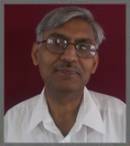
D. K. Sharma
Research Interests
- MOS device modeling
- VLSI design and technology.
- Microelectronics - technology and device characterisation
- mixed signal design
Courses Offered
- EE668 System Design
- EE712 Embedded Systems Design
- EE705 VLSI Design Lab
Academic Background
- M.Sc. from B.I.T.S. Pilani
- Ph.D. from the Tata Institute of Fundamental Research (T.I.F.R.), University of Bombay.
Work Experience
- He was with the Solid State Electronics group at T.I.F.R. during 1971-1991 except for 1976-78, when he was a visiting scientist at L.E.T.I., Grenoble, France and 1985-87, when he was with the Microelectronics Center of North Carolina in the U.S.A. He has been at the Electrical Engineering Department of IIT Bombay since 1991, where he is currently a Professor.
Other Responsibilities
- Member of the editorial board of “Pramana”
Other Information
- He has worked in the areas of technology development, process and device simulation, electro-thermal modeling and characterization of MOS devices. He has 30 papers in these areas. Dr. Sharma maintains close contact with the microelectronics industry in India. He has designed several ICs for the industry, and has conducted training courses for them in the areas of VLSI technology and design.
Contact Information
Department of Electrical Engineering
IIT Bombay, Powai
Mumbai 400 076, India
Email : dinesh[AT]ee.iitb.ac.in
Phone (Internal(O)) : (0091 22) - 2576 7432
Office room no: A202
Fax: (0091 22) - 25723707
faculty/dinesh.txt · Last modified: 2021/09/06 08:38 (external edit)

