AI enabled designing of next-gen photonic devices
26 December 2021 | Shrushti Tapar
I am a researcher working in the domain of nano-electronics within the electrical engineering department at IIT Bombay. The research in this domain mainly contributes to designing, scaling, and thereby enhancing the performance and competence of an electronic chip. In today's digital era, devices, gadgets, and the internet are the most integral part of our daily routines. Worldleading semiconductor companies like TSMC, Intel, Samsung, and GlobalFoundries invest billions of dollars every year on research to keep pace with advancing chip designs for evergrowing data operation speeds. The current chip technology is reaching its limit of possible advancement. I am always curious to know what would be the next paradigm in technology, and this motivated me to look at photonics, which is regarded as an upcoming technology in integrated circuits.
Challenges in developing a new technological paradigm: Electronics versus Photonics
Present computing technology relies on electrons as the fundamental particle carrying information in integrated circuits. Electrons are charged particles, hence their control and manipulation is achieved by the application of different electric and magnetic fields. However, improvement in speed and size of electron-based devices is reaching its limit. Knowing that "Light has an ultimate speed", researchers are trying to achieve data transmission at the speed of light at the level of integrated circuits. So, the idea of using a quanta of light (called photon) for information transfer at the chip-level is referred to as Photonics. The field of photonics is in its infancy. Photons are chargeless entities, thus their confinement, control, and manipulation at spatial and phase level on-chip is challenging.
Background and introduction
The starting point for photonic chips is to bring light on-chip and attain its maneuvering at the nanoscale. Among the possible ways of confining light on the nanoscale, using surface plasmons is an effective technique. Surface plasmons are quanta of oscillations confined at surfaces and have the unique capacity to confine light to very small dimensions. At the nanoscale, the lens, mirrors for manipulating light are replaced by a metasurface. The metasurface is a cleverly engineered dense array of ultra-thin planar nanostructures. Thus, surface plasmons confine light to the chip, and a metasurface attains desired optical response. Before going for actual device fabrication, optimizing the metasurface design parameters for the desired response using simulations is a common practice. In simulations, the way of optimizing nanostructure geometry and parameters is by calculating optical response for each possible combination of design and size and finalizing the nanostructure that is having the closest possible optical response to desired ones. Solving Maxwell’s equations for light-matter interaction for incident light and metasurface using FEM (finite element method) in simulation tools is very expensive in terms of computational resources and time.
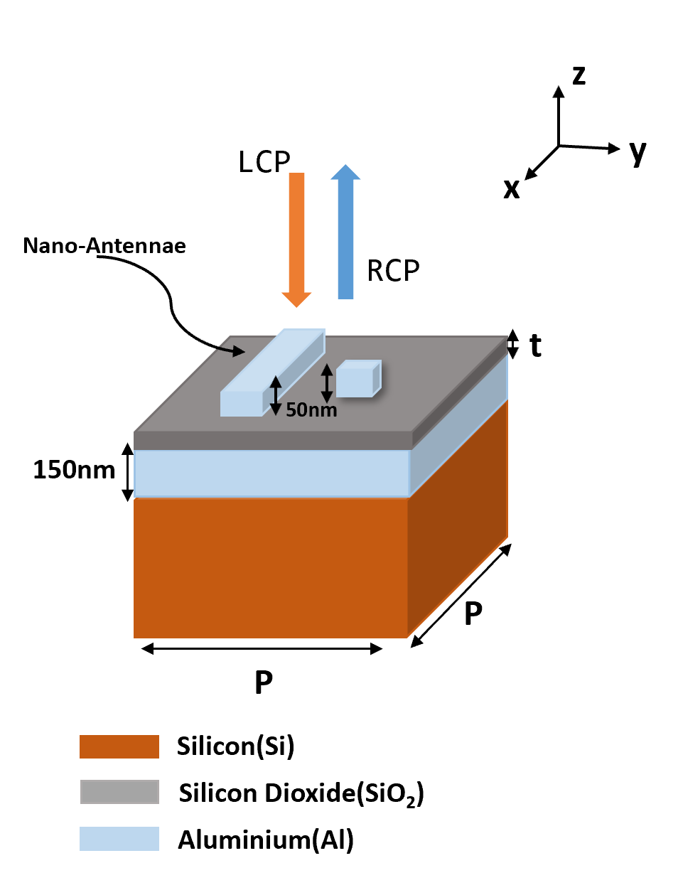
In a recent study by a team led by Prof. Amit Sethi from the electrical engineering department and Prof. Anshuman Kumar from the physics department, researchers have tried to acquire the maximum efficiency of polarization of light by designing a surface plasmon-based metasurface. Polarization efficiency is defined as the percentage of incident light that changes its polarization state (i.e. from right circularly polarized RCP to left circularly polarized LCP and vice versa) on interacting with metasurface at the reflected side. As said before, numerical simulations are an expensive and cumbersome method of obtaining optimized parameters, which the authors tried to overcome by using an AI-based framework.
A schematic illustration of unit cell of gap-plasmon based half-wave plate is shown here.
In to depths
The framework uses Deep Learning (DL) algorithms, which are the subsets of supervised learning. In DL, Neural networks (NN) are trained using data sets (inputs and corresponding outputs) to obtain the output response for new input data without actually solving equations numerically.
Bidirectional Autoencoder (BiAE)
Bidirectional Autoencoder combines the two training stages of NN, the first is encoding, and the second is the decoding stage. The encoding stage is trained for inverse mapping, i.e. generating structural parameters for desired optical response and the decoding stage is trained for forward mapping i.e. for generating optical response for given structural geometry and parameters. The biAE is simultaneously trained for forward and reverse mapping, which improves the performance concerning individually trained networks.
The validation of trained NN is the next stage, where BiAE is validated by comparing the output responses from trained NN with calculated simulation results for randomly picked geometric parameters for each design class, which were not shown during training. The output and calculated response are compared and it was observed that the average mean absolute error is ≤ 5% for 97-100% of the dataset samples.
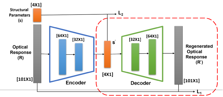
In the training process, the encoder accepts the optical response and produces structural parameters as latent vectors. The decoder then regenerates the optical response from structural parameters.
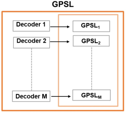
Global library (GPSL)
The Global library is formed by combining many sub-libraries. Each sub-library (GPSL1, GPSL2, GPSLM) corresponds to a particular design class, containing optical responses generated by the decoder for each possible combination of parameters for the provided optical spectrum.
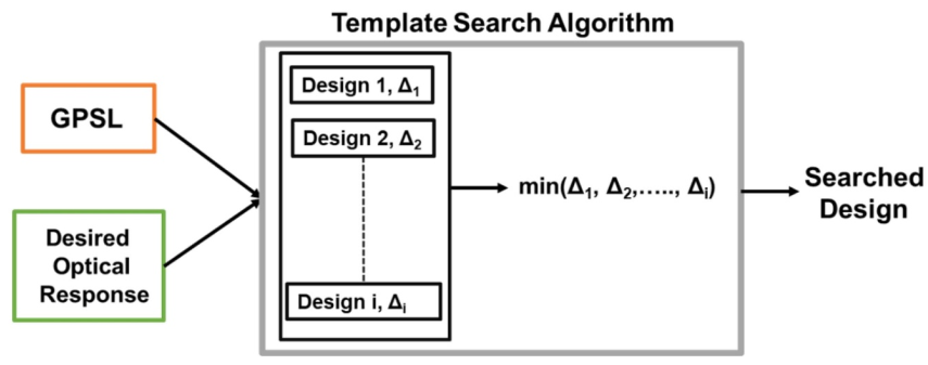
Template search algorithm
Finally, a template search algorithm is used to obtain the optimized design parameters for the closest optical response to the desired response for maximum polarization. Usually, the deep NN faces an issue while working with inverse design mapping, that is having multiple outputs (designs and parameters) for the desired optical response. The proposed template search algorithm addresses this issue and provides the solution in form of local and global optimized design parameters while working at sub-libraries and GPSL levels respectively. The template search algorithm provides non-unique output, multiple designs, and parameter configuration for a desired optical response, that too in duration of milliseconds.
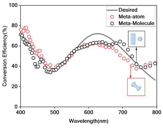
The implemented AI-based algorithm demonstrates that the developed DL architecture accurately and rapidly identifies the optimized structural design and parameters in the space of different metasurface topologies and it can be used for applications needing one to many mapping for inverse design problems.
Research Paper: Abhishek Mall, Abhijeet Patil, Dipesh Tamboli, Amit Sethi, and Anshuman Kumar. "Fast design of plasmonic metasurfaces enabled by deep learning." Journal of Physics D: Applied Physics 53, no. 49 (2020): 49LT01.