Lab Tour - IITBNF
IIT Bombay Nanofabrication Facility (IITBNF)
26 December 2021 | Adil Khan, Pudi Seshasainadh, Janeel Patel
Those who have had a chance to walk along the never-ending pathways of the Infinite Corridor might have seen the tall and sleek nanoelectronics building which houses the IITB Nanofabrication Facility (IITBNF) on its lower levels. However, what many might not be aware of is the amazing research that goes on within the confines of the numerous labs within this facility. Through this article, we aim to take our readers on a quick tour of the IITBNF and provide them with a glimpse of the research work being undertaken inside this state-of-the-art facility.
As stated by IITBNF itself, its guiding mission is to provide a benchmark for state-of-the-art research, learning and outreach in the fields of semiconductor technology and nanotechnology. IITBNF consists of over 18 laboratories under its umbrella and has 60 faculty members associated with it spanning multiple research domains. Such is its importance that even Joe Biden (then the US Vice President) spent two hours touring this facility while on a visit to IIT Bombay in 2013. We would like to especially thank Prof. Udayan Ganguly, a key member and proponent of the IITBNF ecosystem, for sharing a lot of insights on its history and significance with us.
History of IITBNF
Nanofabrication is an integrative and complicated process, with a different set of tools required for each stage of the fabrication process. As Prof. Udayan points out, the culture at IIT Bombay is of setting up shared labs, which are open to researchers across different groups. This is driven by the fact that a large facility such as the IITBNF is beyond what any single faculty member can host alone, and the huge operational requirements for just running such a facility requires collaboration between multiple research groups. IITBNF, together with a similar facility (CeNSE) at IISc form the two earliest pioneers of nanoelectronics research in India.
IITB's journey with device fabrication goes back to 1985 when the first device fabrication lab with a Class 1000 cleanroom was set up through an MHRD funded project on the Centre for Microelectronics. This project was managed jointly by Prof. Juzer Vasi, Prof. A. N. Chandorkar and Prof. R. Lal; who together successfully built a 3 micron NMOS fabrication lab to promote research and teaching in microelectronics. The main boost towards setting up the present day IITBNF came in 2006 with an INR 500 million grant from the Government of India for a collaborative project between IITB and IISc to set up a Centre of Excellence in Nanoelectronics. Many of the cleanrooms, labs and instruments at IITBNF came up between 2006 and 2012 with support obtained from industrial collaborators as well.
Back in 2006, no one expected IITBNF to be a huge success; rather it was more of an aspirational thing. However, fifteen years on, research data today shows that we have done extremely well in nanoelectronics research. A recent article by Prof. Udayan, Sandip Lashkare and Prof. Swaroop published in IEEE Electronic Devices Society Newsletter (January 2021) details the rise of nanoelectronics research in India, led by IIT Bombay. Starting from only a few contributions to nanoelectronics engineering before 2011, we have become one of the top 10 nations in this field, as measured by the number of papers published in IEEE Electronic Devices Letters (EDL) and Transactions on Electronic Devices (TED).
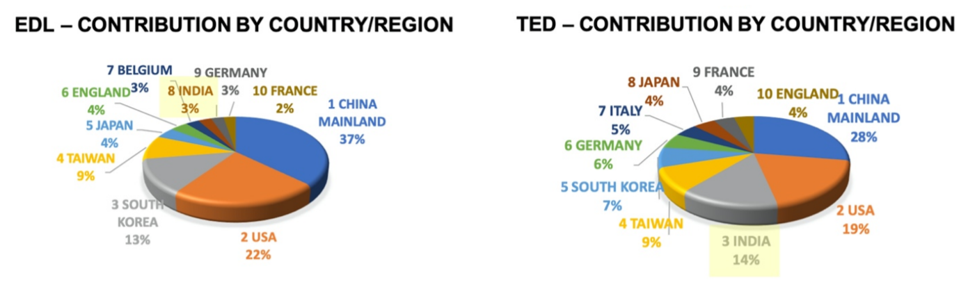
India among the top 10 contributors to research in nanoelectronics in the year 2019
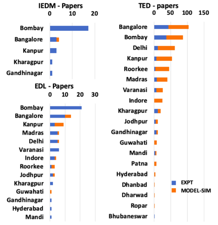
IIT Bombay leads the country in nanoelectronics research as measured by the number of contributions to IEDM, EDL and TED (three eminent publications in this research domain)
Research groups associated with the IITBNF have a large number of industrial collaborations including sponsored projects and fellowships from companies such as Intel, Global Foundries, Applied Materials, IMEC and Micron among numerous others. The establishment of the National Centre on Photovoltaic Research and Education (NCPRE) in 2010 has aided in the expansion of tools and equipment especially in the fields of solar cell research and applications. Through the INUP (Indian Nanoelectronics Users Program), the facilities at IITBNF are also thrown open to the rest of the country, with researchers from other universities and organisations coming here to work on their research proposals and projects.
Areas of Expertise
Research at IITBNF spans numerous technology domains such as computing devices, communication devices and environmental sensors to name a few.
Computing Devices
This has been the traditional area of strength with numerous publications in high-impact journals and conferences and tens of national and international patents. IITBNF houses clean rooms, equipment and process tools for all essential device fabrication processes. Additionally, IITBNF is well-equipped with state-of-the-art device simulation and characterisation facilities, including commercial process tools. Ongoing research in the lab focuses on contemporary topics such as CMOS-based device reliability, advanced CMOS logic devices, advanced memory devices and beyond-CMOS approaches.
Sensing & Actuator Devices
This research domain at IITBNF encompasses a wide range of materials and device platforms that find applications in public health, homeland security and agriculture. Work done in this area is interdisciplinary bringing together groups from Electrical Engineering, Mechanical Engineering, Chemistry and Bio-sciences departments. The facility has full-fledged CAD setups, fabrication tools and characterization facilities for micro/nano electromechanical devices. Some technologies developed here include a point of care sensor for detecting cardiac markers, a handheld device for explosive detection, a wearable web-enabled ECG monitoring device and a soil moisture measurement unit. Prototypes of 320x256 Quantum Dot Infrared Photodetector based IRFPA (infrared photodetectors and focal plane arrays) thermal imagers were developed and demonstrated for the first time in India at IITBNF.
Energy-harvesting Devices
This is a fast-growing, vital area of research attracting immense interest in recent times. IITBNF currently houses 7 laboratories (including a class 1000 cleanroom) exclusively dedicated to solar cell research, which work on modelling, fabrication and characterisation of crystalline, thin film, multi-junction and organic solar cells. Apart from solar energy, the research work at this facility also revolves around deep exploration and evaluation of various other widely available forms of energy to develop energy harvesting devices for numerous electronic applications. Work in this domain is multidisciplinary, bringing together researchers from Energy Science & Engineering, Chemistry and Electrical Engineering departments, among others.
Communication Devices
This research area at IITBNF focuses on relatively new topics such as III-V semiconductors, which are increasingly being deployed for high-speed and high-power applications. IITBNF now possesses state-of-the-art facilities for simulation, characterisation and fabrication of III-V compound semiconductor-based high-speed switches and optoelectronic devices.
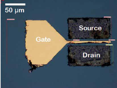
Micrograph of first gallium-nitride HEMT fabricated in India. A gallium nitride (GaN) based high electron mobility transistor (HEMT) was first successfully fabricated in India in 2009 at this facility.
Recent Research
Recently, a 180 nm CMOS based memory technology developed at IITBNF got adopted for indigenous manufacturing by the Semi-Conductor Laboratory, Chandigarh. A team led by Prof. Udayan Ganguly developed this one-time programmable (OTP) memory based on ultra-thin deposited silicon dioxide (a few atoms thick) instead of the existing gate oxide-based OTP technology. In contrast to the high voltage required by current technologies, this new memory chip requires less power and chip-area as the need for boosted voltage supply is avoided. This invention was covered in the national media as well and is considered to be an important national milestone in semiconductor R&D for memory technologies. It enables secure memory and authentication for national products like e-passports and credit cards.
Details of the facilities
Clean Room
It is imperative to have an extremely clean environment for semiconductor fabrication, as the presence of even a tiny dust particle can have a devastating influence on the operation of nanoscale devices. A class 1000 cleanroom, such as that present at IITBNF, has a maximum of 1,000 particles (≥ 0.5 µm in size) per cubic feet of air inside. By comparison, an ordinary room in a building may have more than a million such particles per cubic foot of air.
Lithography
Lithography forms the backbone of a typical semiconductor device fabrication run. It enables one to ‘draw’ or ‘write’ micrometre or nanometre sized patterns, thereby defining the device dimensions. In optical lithography, a UV beam is used for writing, and the pattern sizes can be as small as a few micrometres. Even smaller, nanometre-sized patterns can be written via e-beam lithography which uses a beam of electrons to write. In both cases, 'writing' is done on special light-sensitive (or electron-sensitive) materials known as resists. These are chemically processed after exposure (to the light or electron beam) and reveal the written pattern according to the part that was exposed or left unexposed. IITBNF has multiple optical lithography tools with different pattern dimension limits. The best resolution at IITBNF (< 20 nm) is achieved through a state-of-the-art e-beam lithography tool: RAITH150 Two. For both optical & e-beam tools, mask aligners and resist spinners dedicated to different types of resists are available with capabilities to process 2", 4" and 8" wafers.
Etching Tools
While a lithography process is used to write patterns on a resist layer, a different technique is needed to transfer these patterns from the resist onto the main layer of the semiconductor wafer. Wet etching & dry etching are the most commonly used processes to achieve this goal. IITBNF has separate dry etch tools for silicon and III-V semiconductor samples to prevent material cross-contamination. A general-purpose ion miller is used to dry etch any sample using a purely physical ion bombardment process. Plasma asher tools are also available that are typically used to remove resist from a sample via a chemically reactive oxygen plasma.
Wet Chemistry Tools
Use of chemical solutions is often needed at various stages of device fabrication; most commonly during wafer substrate cleaning and wet etching. In order to minimize cross-contamination and maintain process control, IITBNF has dedicated wet benches and clean stations for silicon placed away from general purpose stations. Complementary apparatus such as sonicators, spin coaters and hot plates are also provided at specific stations.
Deposition, Growth and Anneal Tools
Thin film deposition of some materials is needed at various stages of the process – from the initial active semiconducting layers to the final metal contact layers. With new materials being explored for various applications today, dedicated systems and novel deposition techniques are required to integrate them into devices. Pulsed laser deposition (PLD) and atomic layer deposition (ALD) are two examples of such enabling capabilities available at IITBNF, along with other conventional silicon processing equipment. Apart from these, three molecular-beam epitaxy (MBE) growth systems are available at IITBNF, which can grow different kinds of samples (III-V compounds, III Nitrides, Si, Ge, Sn). MBE works in an ultra-high vacuum and it's slow deposition rate allows the films to grow epitaxially (in an ordered arrangement). For annealing, there are rapid thermal processing (RTP) tools in use with the ability to do annealing, oxidation and nitridation of the substrates as and when required.
Characterisation Tools
IITBNF has an array of physical and chemical characterization tools that enable in-line (during fabrication) and post-fabrication investigation into material structure and related properties. They include optical microscopes, profilometers, ellipsometers and multiple spectroscopy tools. Apart from these, there are extensive facilities for electrical characterisation of nanodevices. Dedicated instruments for detailed measurements and analysis of device capacitance, current, magnetism and lifetime are available. Additionally, instruments for specialized measurements on solar cells and quantum devices are also in place.
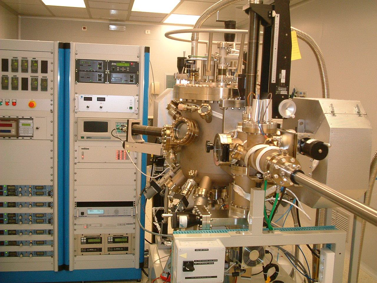
MBE system for GaN at IITBNF
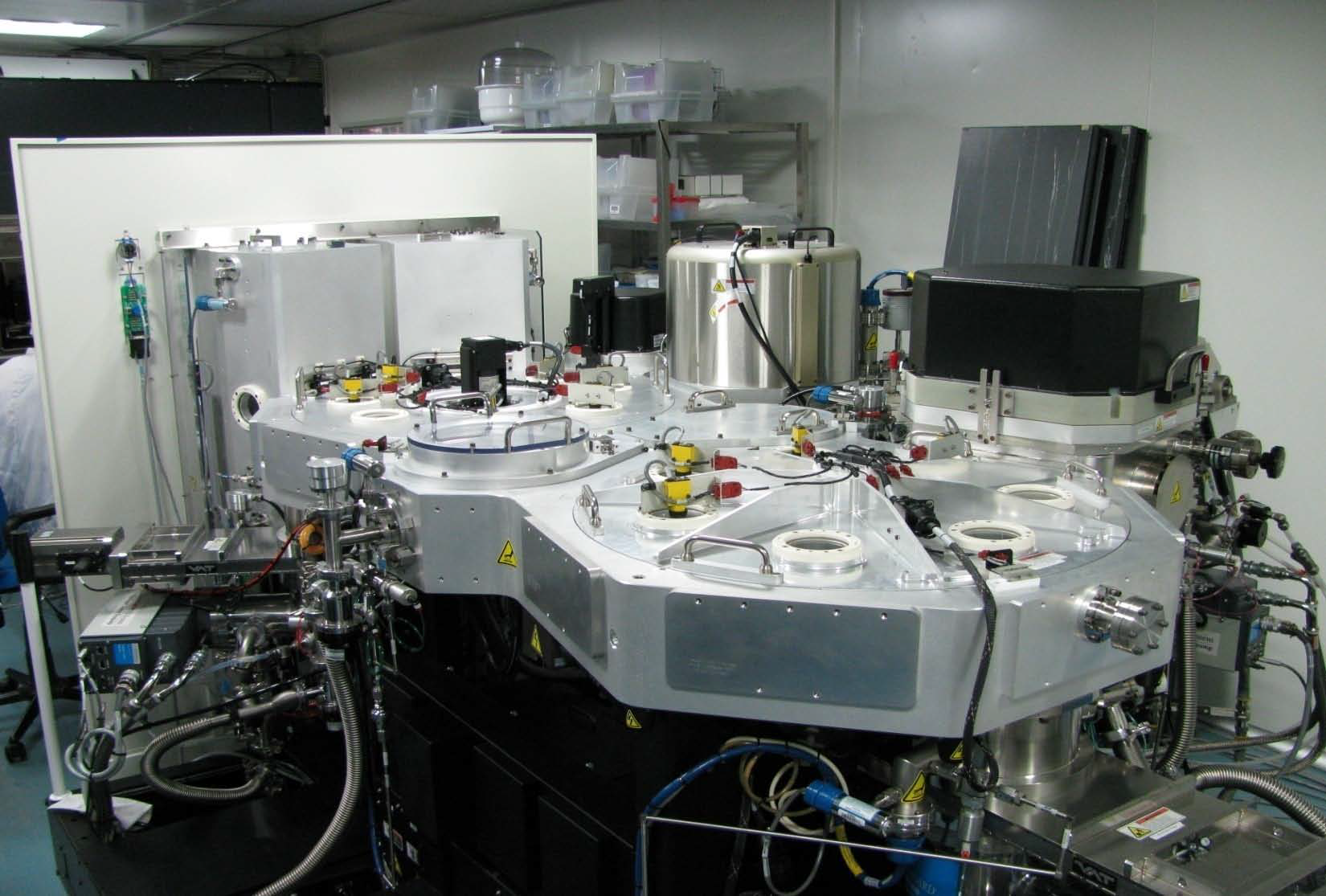
Physical Vapor Deposition system at IITBNF
How to get involved with the work
Prof. Udayan tells us that there are three different kinds of work in which one can get involved at IITBNF. To start with is the simulation-modelling work such as the simulation of new device structures using TCAD software. This is the level of work which is the most accessible to undergraduate students due to their short time constraints. The second level is device characterisation, which includes measuring the electrical, material and structural properties of devices which have already been fabricated. This work is comparatively more time consuming but still feasible for everyone. Then comes the third level which is the actual fabrication of devices. Being a very long and multi stage process, device fabrication is usually carried out by 3-year Masters and PhD students.
The courses that one can do in order to get involved with research at IITBNF include EE735 (Microelectronics Simulation Lab), EE672 (Microelectronics Technology Lab), EE669 (VLSI Technology), EE728 (Growth and Characterization of Nano-electronic Materials) apart from various standard courses on device physics.
Click here to visit the website of IITBNF and find out more about it.