Widening Absorber Bandwidth
Silicon-based absorber bandwidth broadening with bulk processes
26 December 2021 | Karan P Rane
Research work by Ankitha Bangera and Prof. Kumar Appaiah
Material-light interaction
Natural light spectrum can be described as a composition of individual components graphed against a continuum of wavelengths. A spectrometer is used by scientists and engineers to describe the nature of molecules in matter, using the spectrum of light emitted by them. A photodetector is a part of the spectrometer, which converts optical energy into electrical energy.
Light falling on a photodetector is either reflected or transmitted or absorbed. The intensity of the reflected, transmitted and absorbed light depends upon the wavelength of the incident light and the material, silicon surfaces in this article. Characterization is the process employed to measure this dependence on wavelength. Typical silicon based photodetectors have a limited wavelength range (bandwidth). Hence, a complex system consisting of multiple detectors is constructed to sense (or detect) a broad range of frequencies.
Idea for Wider Bandwidth
Ms Ankitha E. Bangera, a researcher at IITB has implemented a process flow for modification of the silicon surface to expand the bandwidth of silicon based photodetectors. These devices absorb photons belonging to a wide spectrum; finding applications in spectrometers, optical noise absorbers and photovoltaic cells. The processes used in the study allow industry-standard bulk manufacturing.
“I was a system owner (incharge of a lab facility) of a spectrometer that used multiple sensors to capture a wider spectrum of light. The requirement of multiple sensors increased the system complexity. This is where the idea to build a wideband device occurred to me”, she said.
Current process: Process flow and testing
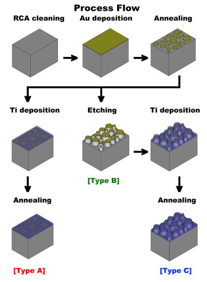
Process flow for three biocompatible configurations is illustrated in the diagram. Type A depicts nanocoating of Ti-compounds (Ti is a symbol for Titanium) formed on Au-islands/ n-Si (Au and Si are the symbols for Gold and Silicon respectively), type B shows Au-island assisted textured n-Si, type C corresponds to nanocoating of Ti-compounds formed on Au-islands/ textured n-Si.
The silicon surface was textured in type B and type C samples because texturing reduces surface reflections.
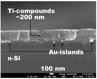
The titanium deposition (Ti of thickness ~ 200 nm), on annealing, forms Ti-Si schottky barrier at the interface and Ti-O and Ti-O-Si hydrophobic surface on the outer surface.
The Schottky barrier improves radiation absorption in the IR region. Hydrophobic surfaces prevent gumming by biological materials. An antireflective coating (such as oxides of Ti formed on the surface) or a textured (textured-Si) surface reduces the noise which fortifies the configurations against multiple types of degradation.
Potential Applications
The three biocompatible configurations reduce surface reflections and improve the absorbance for silicon surfaces over an ultra-wideband region of wavelength ranging from UV to IR. These configurations can find applications in broadband absorbers, anti-reflective surfaces and optical detectors or sensors for spectroscopy. The fabrication steps are non-lithographic, which can lead to cost effective bulk manufacturing in industries. The surface hydrophobicity of type A and type C configurations allow integration with biological devices.
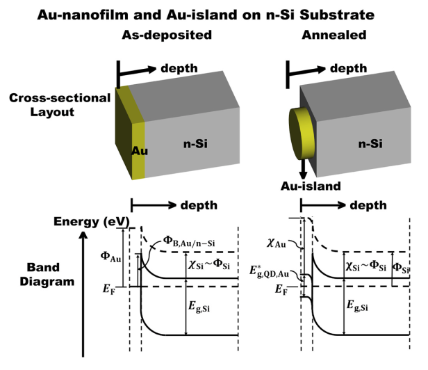
The energy band gap is the energy required by an electron to transition from valence band to conduction band.
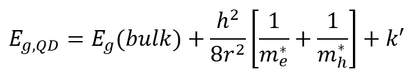
The above expression tells us how the radius of the Au(Gold)-island, r affects the band gap.
The band gap for a large Au-island goes to zero as r in the expression increases, but for small islands, the band gap widens as r diminishes. Depending on the size of the island formed, radiation in a certain range of spectrum is absorbed by the surface.
Cross sectional SEM image confirms thickness of Ti-compounds and presence of Au-islands. The XPS wide scan confirms the surface chemical composition, which comprises Ti–O on the surface of the samples
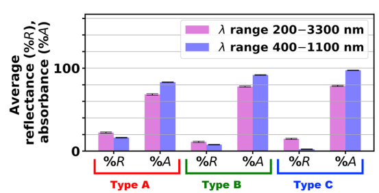
Type A involves blanket deposition and annealing processes whereas type B and type C involve an additional process for surface texturing.
Type C provides least average reflectance ~2% and highest average absorbance ~97%, for wavelengths ranging from 400 nm to 1100 nm.
Challenges Encountered and Overcome
Timing is a key requirement of the modification process. When exposed to air, silicon surfaces form native oxide. Hence, the deposition steps need to be done quickly, say, within a day or two. Storing the samples in a vacuum desiccator before the deposition avoids silicon surface oxidation.
After the final samples are prepared, the modified surfaces, that consist of nanocoatings of Ti-compounds, act as a passivation, even though the samples are not stored in a vacuum desiccator. A similar challenge related to timing lies in the process of etching, which requires careful monitoring. All facilities required for fabrication were available on campus. However, the pace of study is limited by the availability of target elements.
Conclusion
The proposed configurations reduce surface reflections and enhance absorbance for silicon surfaces over an ultra-wideband region. The processes used in fabrication allow cost-effective bulk manufacturing in industries. All the materials used are biocompatible, eco-friendly and non-toxic. Schottky and quantum effects due to Au gold islands are demonstrated. Surface hydrophobicity in Titanium coated surfaces can benefit in integration with biological devices for human implants.
Research Paper: Bangera, A. E., & Appaiah, K. (2021). Quantum-confined ultra-wideband Si-based absorbers by a non-lithographic approach. Solar Energy Materials and Solar Cells, 230, 111161.