H/W 5: Introduction to AVRMicrocontroller (ATmega 16/32)
1. Part A: Theory
Read through the following material.
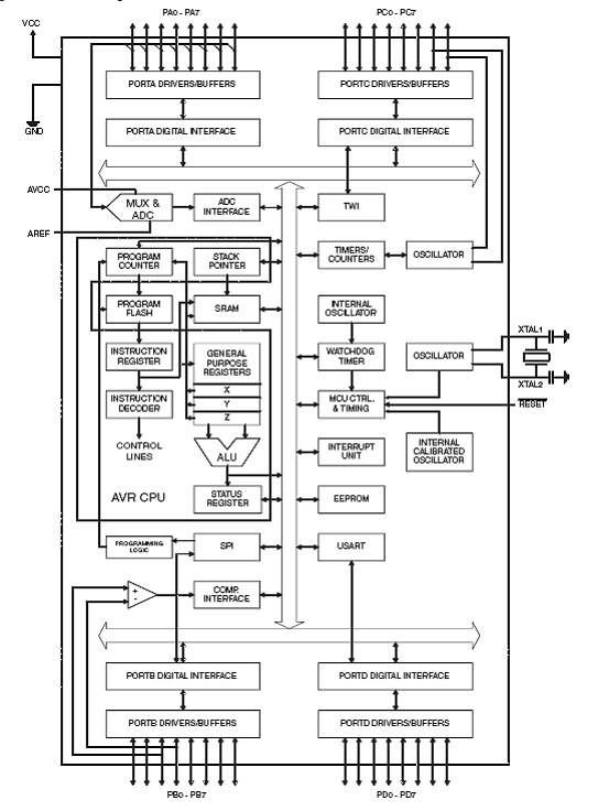
Features of ATmega 16 (AVR Microcontrollers)
• Advanced RISC Architecture (Harvard architecture support
– 131 Powerful Instructions – Most Single-clock Cycle Execution
– 32 x 8 General Purpose Working Registers
– Up to 16 MIPS Throughput at 16 MHz
• High Endurance Non-volatile Memory segments
– 16K Bytes of In-System Self-programmable Flash program memory
– 512 Bytes EEPROM
– 1K Byte Internal SRAM
– Optional Boot Code Section with Independent Lock Bits
In-System Programming by On-chip Boot Program
• JTAG (IEEE std. 1149.1 Compliant) Interface
– Boundary-scan Capabilities According to the JTAG Standard
– Extensive On-chip Debug Support
– Programming of Flash, EEPROM, Fuses, and Lock Bits through the JTAGInterface
• Peripheral Features
– Two 8-bit Timer/Counters with Separate Prescalers and Compare Modes
– One 16-bit Timer/Counter with Separate Prescaler, Compare Mode, andCapture Mode
– Real Time Counter with Separate Oscillator
– Four PWM Channels
– 8-channel, 10-bit ADC
– Byte-oriented Two-wire Serial Interface
– Programmable Serial USART
– Master/Slave SPI Serial Interface
– Programmable Watchdog Timer with Separate On-chip Oscillator
– On-chip Analog Comparator
• Special Microcontroller Features
– Power-on Reset and Programmable Brown-out Detection
– Internal Calibrated RC Oscillator
– External and Internal Interrupt Sources
– Sleep Modes for Power Conservation: Idle, ADC Noise Reduction, Power-save,Power-down, Standby, Extended Standby
• I/O and Packages
– 32 Programmable I/O Lines
Problemstatement:
Interface a keyboard (at PORTA) with the AVR ATmega 32 Microcontroller tocontrol the intensity of the LED connected(at PORTD pin5) at its output by 16steps (using PWM) and simultaneously send the data of Pulse WidthModulation/key pressed to the PC using a serial communication interface(usingPORTD pins 0 and 1).
Circuit Diagram
Stage 1:
Implement the Serial communication interface using MAX232 IC and fewpassive components.
Check if this part of the circuit is functioning properly
Test:
Short the T1IN and R1OUT pins to observe if loop-back of the data isproper and without errors.
*Loop-back – connect the DB9 connector between the PC and MAX232 IC;send the data using hyper-terminal or any other serial port monitoringsoftware. Observe if the data sent on the Serial port is reflected back.
Stage 2:
Check if the Boot-loader burned into the microcontroller is functioningproperly.
Procedure:
·
·
·
·
Stage 3:
Configure the ports of Atmega32 to either input or output modedepending on the specifications.
Configure the port for keyboard interface as per requirements (half of theport as input and half of the port as output as same logic is used for 8051.)
Step run and simulate this program using AVRSTUDIO.
Stage 4:
Configure the serial port of the microcontroller for communication atbaud rate 9600, 8bits data, no parity bit and 1 stop bit, asynchronous mode.
Supporting Registers
UCSRA=0xpq;
UCSRB=0xrs;
UCSRC=0xtu;
UBRR
UBRR= ![]()
We have set ![]() to 8MHz(internal RC oscillator) in the fuse bit settings.
to 8MHz(internal RC oscillator) in the fuse bit settings.
USARTControl and Status Register A – UCSRA
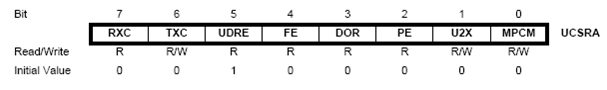
•Bit 7 – RXC: USART Receive Complete
Thisflag bit is set when there are unread data in the receive buffer and clearedwhen receive buffer is empty (i.e., does not contain any unread data). If thereceiver is disabled, the receive buffer will be flushed and consequently theRXC bit will become zero. The RXC Flag can be used to generate a ReceiveComplete interrupt (see description of the RXCIE bit).
•Bit 6 – TXC: USART Transmit Complete
Thisflag bit is set when the entire frame in the transmit Shift Register has beenshifted out and there are no new data currently present in the transmit buffer(UDR). The TXC Flag bit is automatically cleared when transmit completeinterrupt is executed, or it can be cleared by writing a one to its bitlocation. The TXC Flag can generate a Transmit Complete interrupt (seedescription of the TXCIE bit).
•Bit 5 – UDRE: USART Data Register Empty
TheUDRE Flag indicates if the transmit buffer (UDR) is ready to receive new data.If UDRE is one, the buffer is empty, and therefore ready to be written. TheUDRE Flag can generate a Data Register empty Interrupt (see description of theUDRIE bit). UDRE is set after a reset to indicate that the transmitter isready.
•Bit 4 – FE: Frame Error
Thisbit is set if the next character in the receive buffer had a Frame Error whenreceived. i.e., when the first stop bit of the next character in the receivebuffer is zero. This bit is valid until the receive buffer (UDR) is read. TheFE bit is zero when the stop bit of received data is one. Always set thisbit to zero when writing to UCSRA.
•Bit 3 – DOR: Data Overrun
Thisbit is set if a Data Overrun condition is detected. A Data Overrun occurs whenreceive buffer is full (two characters), it is a new character waiting in thereceive Shift Register, and a new start bit is detected. This bit is validuntil the receive buffer (UDR) is read. Always set this bit to zero whenwriting to UCSRA.
•Bit 2 – PE: Parity Error
Thisbit is set if the next character in the receive buffer had a Parity Error whenreceived and the parity checking was enabled at that point (UPM1 = 1). This bitis valid until the receive buffer
(UDR)is read. Always set this bit to zero when writing to UCSRA.
•Bit 1 – U2X: Double the USART Transmission Speed
Thisbit only has effect for the asynchronous operation. Write this bit to zero whenusing synchronous operation.
Writingthis bit to one will reduce the divisor of the baud rate divider from 16 to 8effectively doubling the transfer rate for asynchronous communication.
•Bit 0 – MPCM: Multi-processor Communication Mode
Thisbit enables the Multi-processor Communication mode. When the MPCM bit is writtento one, all the incoming frames received by the USART receiver that do notcontain address information will be ignored. The transmitter is unaffected bythe MPCM setting.
USARTControl and Status Register B – UCSRB
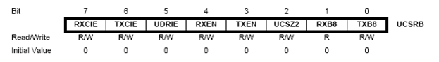
•Bit 7 – RXCIE: RX Complete Interrupt Enable
Writingthis bit to one enables interrupt on the RXC Flag. A USART Receive CompleteInterrupt will be generated only if the RXCIE bit is written to one, the GlobalInterrupt Flag in SREG is written to one and the RXC bit in UCSRA is set.
•Bit 6 – TXCIE: TX Complete Interrupt Enable
Writingthis bit to one enables interrupt on the TXC Flag. A USART Transmit CompleteInterrupt will be generated only if the TXCIE bit is written to one, the GlobalInterrupt Flag in SREG is written to one and the TXC bit in UCSRA is set.
•Bit 5 – UDRIE: USART Data Register Empty Interrupt Enable
Writingthis bit to one enables interrupt on the UDRE Flag. A Data Register EmptyInterrupt will be generated only if the UDRIE bit is written to one, the GlobalInterrupt Flag in SREG is written to one and the UDRE bit in UCSRA is set.
•Bit 4 – RXEN: Receiver Enable
Writingthis bit to one enables the USART Receiver. The Receiver will override normalport operation for the RxD pin when enabled. Disabling the Receiver will flushthe receive buffer invalidating the FE, DOR, and PE Flags.
•Bit 3 – TXEN: Transmitter Enable
Writingthis bit to one enables the USART Transmitter. The Transmitter will overridenormal port operation for the TxD pin when enabled. The disabling of theTransmitter (writing TXEN to zero) will not become effective until ongoing andpending transmissions are completed, i.e., when the transmit Shift Register andtransmit Buffer Register do not contain data to be transmitted. When thetransmitter is disabled, the transmitter will no longer override the TxD port.
•Bit 2 – UCSZ2: Character Size
TheUCSZ2 bits combined with the UCSZ1:0 bit in UCSRC sets the number of data bits(Character Size) in a frame the receiver and transmitter use.
•Bit 1 – RXB8: Receive Data Bit 8
RXB8is the ninth data bit of the received character when operating with serialframes with nine data bits. This bit must be read before reading the low bitsfrom UDR.
•Bit 0 – TXB8: Transmit Data Bit 8
TXB8is the ninth data bit in the character to be transmitted when operating withserial frames with nine data bits. This bit must be written before writing thelow bits to UDR.
USARTControl and Status Register C – UCSRC

•Bit 7 – URSEL: Register Select
Thisbit selects between accessing the UCSRC or the UBRRH Register. It is read asone when reading UCSRC. The URSEL must be one when writing the UCSRC.
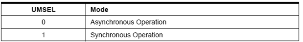
•Bit 6 – UMSEL: USART Mode Select
Thisbit selects between Asynchronous and Synchronous mode of operation.
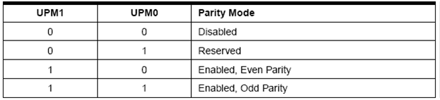
•Bit 5:4 – UPM1:0: Parity Mode
Thesebits enable and set type of parity generation and check. If enabled, thetransmitter will automatically generate and send the parity of the transmitteddata bits within each frame. The
Receiverwill generate a parity value for the incoming data and compare it to the UPM0setting.
Ifa mismatch is detected, the PE Flag in UCSRA will be set.
•Bit 3 – USBS: Stop Bit Select
Thisbit selects the number of Stop Bits to be inserted by the Transmitter. TheReceiver ignores this setting.
UMSEL Bit Settings
UPM Bits Settings

USBS Bit Settings
• Bit 2:1 – UCSZ1:0: Character Size
The UCSZ1:0 bits combined with the UCSZ2 bit in UCSRB sets thenumber of data bits (Character
Size) in a frame the Receiver and Transmitter use.
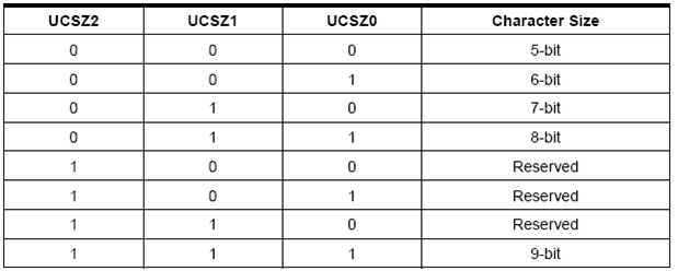
UCSZ Bits Settings
• Bit 0 – UCPOL: Clock Polarity
This bit is used for Synchronous mode only. Write this bit to zerowhen Asynchronous mode is used. The UCPOL bit sets the relationship betweendata output change and data input sample, and the synchronous clock (XCK).
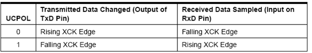
UCPOL Bit Settings
USART Baud Rate Registers – UBRRL and UBRRH
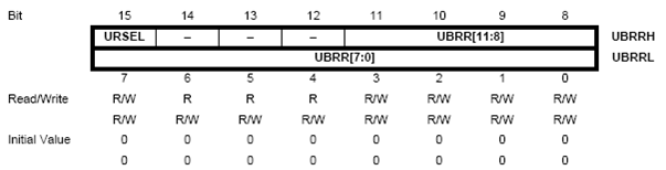
• Bit 15 – URSEL: Register Select
This bit selects between accessing the UBRRH or the UCSRC Register.It is read as zero when reading UBRRH. The URSEL must be zero when writing theUBRRH.
• Bit 14:12 – Reserved Bits
These bits are reserved for future use. For compatibility withfuture devices, these bits must be written to zero when UBRRH is written.
•Bit 11:0 – UBRR11:0: USART Baud Rate Register
Thisis a 12-bit register which contains the USART baud rate. The UBRRH contains thefour most significant bits, and the UBRRL contains the 8 least significant bitsof the USART baud rate. Ongoing transmissions by the transmitter and receiverwill be corrupted if the baud rate is changed. Writing UBRRL will trigger animmediate update of the baud rate Prescaler.
Execute the program in step-run mode in AVRSTUDIO and check if thereceiving and transmitting parts of the program work properly (andindependently).
Flash/Burn the code in the microcontroller and check the same. (One ofthe methods to check if the code is working properly could be receiving thedata serially and transmitting 1 + received data back to the PC
E.g.:
| Sequence number | computer | microcontroller | Direction |
| 1 | a->->->->->->->-> | ->->->->->->->->a | Computer to microcontroller |
| 2 | (a+1)<-<-<-<-<-<- | <-<-<-<-<-<-(a+1) | Microcontroller to computer |
Stage 5:
Timer/Counter1Control Register A – TCCR1A
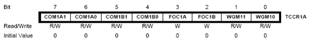
• Bit 7:6 – COM1A1:0: Compare Output Mode for Channel A
• Bit 5:4 – COM1B1:0: Compare Output Mode for Channel B
The COM1A1:0 and COM1B1:0 control the Output Compare pins (OC1A andOC1B respectively) behavior. If one or both of the COM1A1:0 bits are written toone, the OC1A output overrides the normal port functionality of the I/O pin itis connected to. If one or both of the COM1B1:0 bit are written to one, theOC1B output overrides the normal port functionality of the I/O pin it isconnected to. However, note that the Data Direction Register (DDR) bitcorresponding to the OC1A or OC1B pin must be set in order to enable the outputdriver.
When the OC1A or OC1B is connected to the pin, the function of theCOM1x1:0 bits is dependent of the WGM13:0 bits setting.
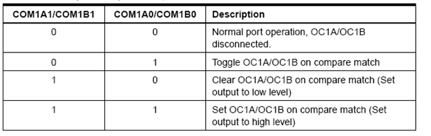
Compare Output Mode, non-PWM
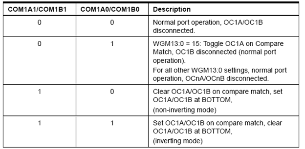
Compare Output Mode, Fast PWM
• Bit 3 – FOC1A: Force Output Compare for Channel A
• Bit 2 – FOC1B: Force Output Compare for Channel B
The FOC1A/FOC1B bits are only active when the WGM13:0 bitsspecifies a non-PWM mode.
However, for ensuring compatibility with future devices, thesebits must be set to zero when
TCCR1A is written when operating in a PWM mode. When writing alogical one to the
FOC1A/FOC1B bit, an immediate compare match is forced on theWaveform Generation unit.
The OC1A/OC1B output is changed according to its COM1x1:0 bitssetting. Note that the
FOC1A/FOC1B bits are implemented as strobes. Therefore it is thevalue present in the
COM1x1:0 bits that determine the effect of the forced compare.
A FOC1A/FOC1B strobe will not generate any interrupt nor will itclear the timer in Clear Timer on Compare match (CTC) mode using OCR1A as TOP.
The FOC1A/FOC1B bits are always read as zero.
• Bit 1:0 – WGM11:0: Waveform Generation Mode
Combined with the WGM13:2 bits found in the TCCR1B Register, thesebits control the counting sequence of the counter, the source for maximum (TOP)counter value, and what type of waveform generation to be used, Modes ofoperation supported by the Timer/Counter unit are: Normal mode (counter), ClearTimer on Compare match (CTC) mode, and three types of Pulse Width Modulation(PWM) modes.
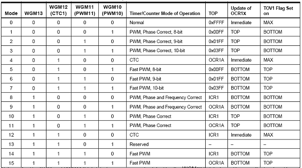
Waveform Generation Mode Bit Description(1)
Timer/Counter1Control Register B – TCCR1B
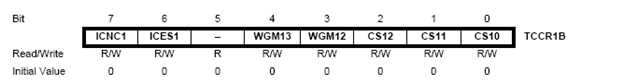
• Bit 7 – ICNC1: Input Capture Noise Canceller
Setting this bit (to one) activates the Input Capture NoiseCanceller. When the Noise Canceller is activated, the input from the InputCapture Pin (ICP1) is filtered. The filter function requires four successiveequal valued samples of the ICP1 pin for changing its output. The Input Captureis therefore delayed by four Oscillator cycles when the Noise Canceller isenabled.
• Bit 6 – ICES1: Input Capture Edge Select
This bit selects which edge on the Input Capture Pin (ICP1) that isused to trigger a capture event. When the ICES1 bit is written to zero, afalling (negative) edge is used as trigger, and when the ICES1 bit is writtento one, a rising (positive) edge will trigger the capture.
When a capture is triggered according to the ICES1 setting, thecounter value is copied into the
Input Capture Register (ICR1). The event will also set the InputCapture Flag (ICF1), and this can be used to cause an Input Capture Interrupt,if this interrupt is enabled.
When the ICR1 is used as TOP value (see description of the WGM13:0bits located in the TCCR1A and the TCCR1B Register), the ICP1 is disconnectedand consequently the Input Capture function is disabled.
• Bit 5 – Reserved Bit
This bit is reserved for future use. For ensuring compatibilitywith future devices, this bit must be written to zero when TCCR1B is written.
• Bit 4:3 – WGM13:2: Waveform Generation Mode
See TCCR1A Register description.
• Bit 2:0 – CS12:0: Clock Select
The three Clock Select bits select the clock source to be used bythe Timer/Counter
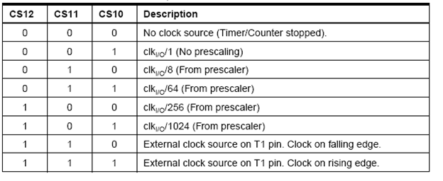
Clock Select Bit Description
If external pin modes are used for the Timer/Counter1, transitionson the T1 pin will clock the counter even if the pin is configured as anoutput. This feature allows software control of the counting.
Timer/Counter1– TCNT1H and TCNT1L
The two Timer/Counter I/O locations (TCNT1H and TCNT1L,combined TCNT1) give direct access, both for read and for write operations, tothe Timer/Counter unit 16-bit counter. To ensure that both the high and Low bytesare read and written simultaneously when the CPU accesses these registers, theaccess is performed using an 8-bit temporary High Byte Register (TEMP). Thistemporary register is shared by all the other 16-bit registers.
Modifying the counter (TCNT1) while the counter is runningintroduces a risk of missing a compare match between TCNT1 and one of the OCR1xRegisters.
Writing to the TCNT1 Register blocks (removes) the compare matchon the following timer clock for all compare units.
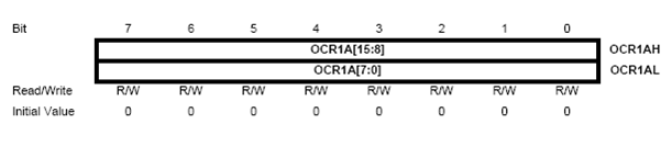
OutputCompare Register 1 A – OCR1AH and OCR1AL
OutputCompare Register 1 B – OCR1BH and OCR1BL
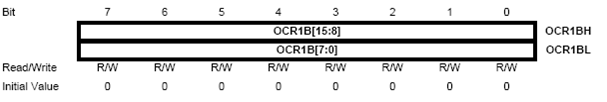
TheOutput Compare Registers contain a 16-bit value that is continuously comparedwith the counter value (TCNT1). A match can be used to generate an outputcompare interrupt, or to generate a waveform output on the OC1x pin.
TheOutput Compare Registers are 16-bit in size. To ensure that both the high and Lowbytes are written simultaneously when the CPU writes to these registers, theaccess is performed using an 8-bit temporary High Byte Register (TEMP). Thistemporary register is shared by all the other 16-bit registers.
Timer/Counter Interrupt Mask Register – TIMSK
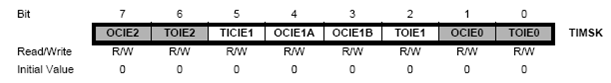
• Bit 5 – TICIE1: Timer/Counter1, Input Capture Interrupt Enable
When this bit is written to one, and the I-flag in the StatusRegister is set (interrupts globally enabled), the Timer/Counter1 Input CaptureInterrupt is enabled. The corresponding Interrupt
Vector is executed when the ICF1 Flag, located in TIFR, is set.
• Bit 4 – OCIE1A: Timer/Counter1, Output Compare A Match InterruptEnable
When this bit is written to one, and the I-flag in the StatusRegister is set (interrupts globally enabled), the Timer/Counter1 OutputCompare A match interrupt is enabled. The corresponding Interrupt Vector is executed when the OCF1A Flag, located in TIFR, is set.
• Bit 3 – OCIE1B: Timer/Counter1, Output Compare B Match InterruptEnable
When this bit is written to one, and the I-flag in the StatusRegister is set (interrupts globally enabled), the Timer/Counter1 OutputCompare B match interrupt is enabled. The corresponding Interrupt Vector isexecuted when the OCF1B Flag, located in TIFR, is set.
• Bit 2 – TOIE1: Timer/Counter1, Overflow Interrupt Enable
When this bit is written to one, and the I-flag in the StatusRegister is set (interrupts globally enabled), the Timer/Counter1 OverflowInterrupt is enabled. The corresponding Interrupt Vector is executed when theTOV1 Flag, located in TIFR, is set.
Timer/CounterInterrupt Flag Register – TIFR
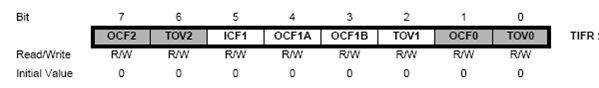
• Bit 5 – ICF1: Timer/Counter1, Input Capture Flag
This flag is set when a capture event occurs on the ICP1 pin. Whenthe Input Capture Register (ICR1) is set by the WGM13:0 to be used as the TOPvalue, the ICF1 Flag is set when the counter reaches the TOP value.
ICF1 is automatically cleared when the Input Capture InterruptVector is executed. Alternatively, ICF1 can be cleared by writing a logic oneto its bit location.
• Bit 4 – OCF1A: Timer/Counter1, Output Compare A Match Flag
This flag is set in the timer clock cycle after the counter(TCNT1) value matches the Output Compare Register A (OCR1A).
Note that a Forced Output Compare (FOC1A) strobe will not set theOCF1A Flag.
OCF1A is automatically cleared when the Output Compare Match AInterrupt Vector is executed. Alternatively, OCF1A can be cleared by writing alogic one to its bit location.
• Bit 3 – OCF1B: Timer/Counter1, Output Compare B Match Flag
This flag is set in the timer clock cycle after the counter(TCNT1) value matches the Output Compare Register B (OCR1B).
Note that a forced output compare (FOC1B) strobe will not set theOCF1B Flag.
OCF1B is automatically cleared when the Output Compare Match BInterrupt Vector is executed.
Alternatively, OCF1B can be cleared by writing a logic one to itsbit location.
• Bit 2 – TOV1: Timer/Counter1, Overflow Flag
The setting of this flag is dependent of the WGM13:0 bits setting.In normal and CTC modes, the TOV1 Flag is set when the timer overflows.
TOV1 is automatically cleared when the Timer/Counter1 Overflowinterrupt vector is executed.
Alternatively, TOV1 can be cleared by writing a logic one to itsbit location.
Stage 6:
Hard code the PWM pulse width and ensure that the PWM output varies theintensity of the led connected at port pin.
Stage 7:
Implement logic to detect a key press event on the matrix keyboard.
(a) Key- Detection:
The key-detection principle is as shown in the following figure.
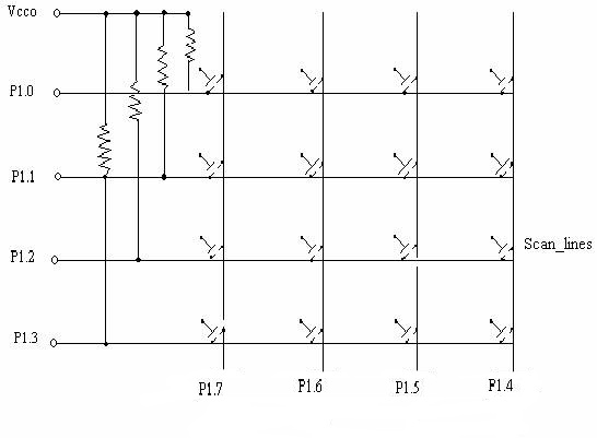
Algorithm:
1. Make sure all the keys are in released state.
2. Poll for key-press event. (Listen if any key is pressed at all.)
3. Ground a ground_line
4. Scan/ read all the scan-lines.
5. Scan_line being LOW implies the key-press at the correspondingjunction of scan_line & ground_line.
6. If scan_line is HIGH, continue the search in similar manner.
(b) Debouncing of keys: (Optional)
Key-stroke events cause a jitter in the electric signal generated bykey_press & key_release events. One needs to wait for a period called‘debounce-delay’ for jitter to die- out & obtain a reliable voltage level.
Procedure:
Write the code for 4*4 key-pad interface & enter the code. Writethe look-up table in lieu with the port- pin connections on theport-tap-out card. Test all the keys.
Hint:
(Similar procedure in Assembly language):
From the write-up study following instructions carefully
mov dptr, #xxxx;
mov p1, #xx;
cjne;
djnz;
clr;
setb;
movx;
jb;
jnb;
mov REG, #xx.
Configure the port pins as Input or Output or Input and Output. Write alogic on to the port pin/s and then scan the rest of the port pin/s.
Stage 8:
Extend the logic to find which key was pressed.
This includes polling of the port pins by sending various combinationallogics on the pins configured as output and scanning the pins which areconfigured as input.
Stage 9:
Whenever a key is detected, send the ASCII code of the key pressed bythe user to the serial port data register.
Stage 10:
Assign fixed pulse width values to each key and also update the PWMwaveform width at each key press events.
Tools and Equipments
Presentation file:
AVR_AID for
CODEVISION AVR evaluation version:
http://www.hpinfotech.ro/html/download.htm
WINAVR
http://sourceforge.net/projects/winavr/files
AVR STUDIO
http://www.atmel.com/dyn/Products/tools_card.asp?tool_id=2725
Megaload
To burn the program into the microcontroller using serial portinterface
ATMega32 Datasheet
http://www.atmel.com/dyn/resources/prod_documents/doc2503.pdf
Serial Port Communication Tool
Reference Books:
" Programming and Customizing the AVR Microcontroller" by Dhananjay Gadre
"Embedded C Programming and the Atmel AVR" by Richard H. Barnett, P.E., Ph.D.; Sarah Cox; Larry O'Cull