Overview of Research Interest:
As our community seeks to advance the performance and size of electronic devices in line with Moore’s law, device sizes are shrinking to nanometer dimensions, and in a few decades, will reach extreme dimensions at atomic scales. This necessitates a paradigm shift if progress is to continue at a rate that has been benchmarked by the semiconductor revolution. In response to this challenge, multiple research groups across many universities, national laboratories and private companies across the world are devoted to the challenges of designing and fabricating functional and reliable devices at atomic size scales, thanks to the boom in nanotechnology. As we scale down to these domains, we must shun our intuitive insights and embrace quantum physics that dictates the behaviour of these tiny objects.
In this context, diamond has emerged as a promising material for solid-state quantum optics and other applications due to the presence of optically active point defects or so-called color centers. In particular, the negatively charged nitrogen-vacancy (NV), and silicon-vacancy (SiV) centers provide electronic and nuclear spins, which can be initialized, manipulated and read out via optical and microwave fields. This platform not only provides the opportunity to explore a wide variety of sensor-related applications but also investigate several unsolved fundamental questions.
Research Areas:
- Hybrid quantum systems – microwave and photonic cavities coupled to color defect
- Quantum sensing and imaging with NV-centers in diamond
- condensed-matter systems
- biological systems
- Portable quantum sensors
- Development of FPGAs for quantum control and other peripheral devices
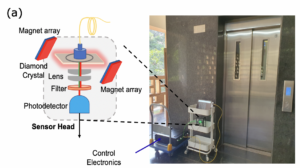
Miniaturisation of NV diamond based magnetic field sensors
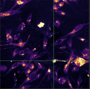
Bio-molecular sensing using nano-diamonds
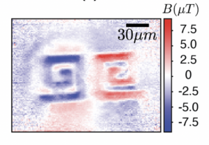
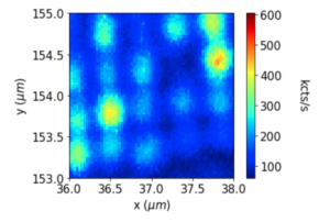
Quantum diamond microscopy: We build magnetic microscopes to investigate semiconductor microchips and explore fundamental physics in various 2D ferromagnetic materials via mapping of magnetic fields and current densities with high patio-temporal resolution.
Quantum information processing: We design and fabricate photonic structures on diamond for single photon generation, hybrid quantum devices and quantum memories.
Note for Prospective Students:
P-QuEST Lab will provide you opportunities of working at the crossroad of exciting and practical applications at the intersection of quantum physics, photonics, and micro- and nano-fabricated sensors. In particular, research will have a focus on design, simulations, fabrication, building experimental setups and characterization involving MW, RF and photonic devices.
Students seeking to work with the P-QuEST Lab must have good analytical skills and be able to find creative solutions to a variety of problems. Course background and a good understanding of electrostatics and dynamics, optics, and hands-on knowledge of electronic circuits and coding are essential for succeeding in our group. There are openings for interested students with suitable backgrounds in multiple roles spanning fabrication, design, and simulation, programming, and instrumentation. Prospective students can contact me to set up an appointment to discuss opportunities. There are project openings for Ph.D. students, B.Tech., M.Tech., and D.D. students as well.