Printed Circuit Board (PCB) Fabrication Laboratory

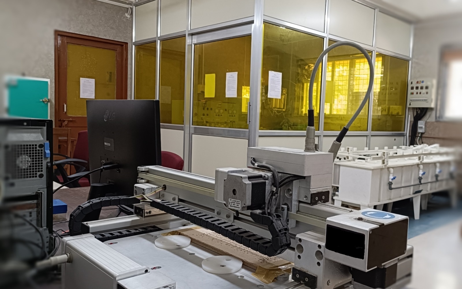
PCB lab provides a facility for printed circuit boards (PCBs) for various electronic applications. The lab includes equipment and machines to fabricate printed circuit boards (PCBs) and it offers fabrication services for both single and double-sided PCBs.

Please read the PCB LABs 'Instruction Manual' and 'Minimum Design Requirement Manual' before requesting pcb fabrication from the PCB LAB.

  • Instruction Manual -> View
  • Minimum Design Requirement Manual -> View
  • Kindly fill in the required information on the Job Order Form and submit it in person to the PCB Lab to request the fabrication of your PCB.

  • PCB Job Order Form -> View
  • Access detailed specifications for single-sided and double-sided FR4 materials.

  • Single-Sided copper clad laminate datasheet -> View
  • Double-Sided copper clad laminate datasheet -> View
  • Image 1
    Bare Copper PCB

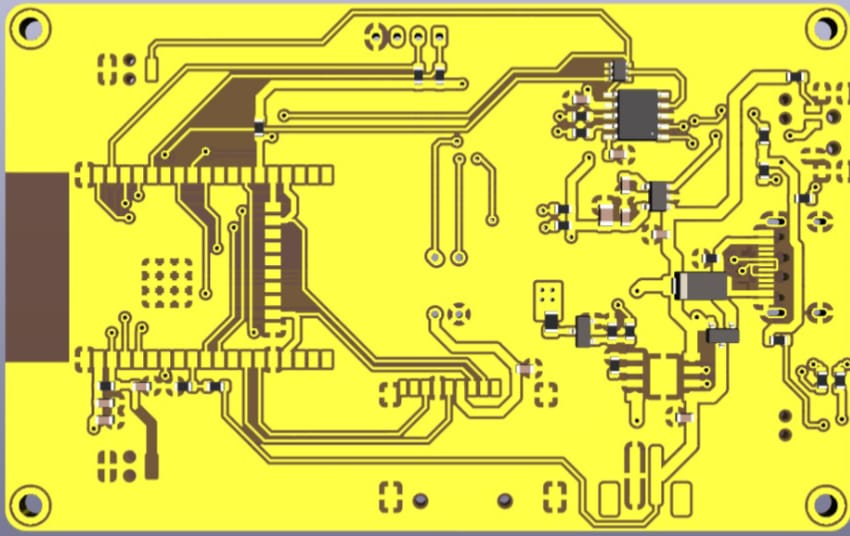
    PCB board without Soldermask and Legend-Printing or Silkscreen option.

    Image 1
    PCB with Soldermask and Silkscreen

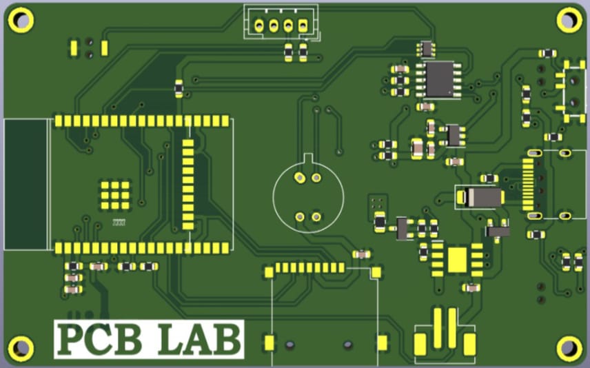
    PCB board with Soldermask and Legend-Printing or Silkscreen option.

    Image 1
    Photo-Film

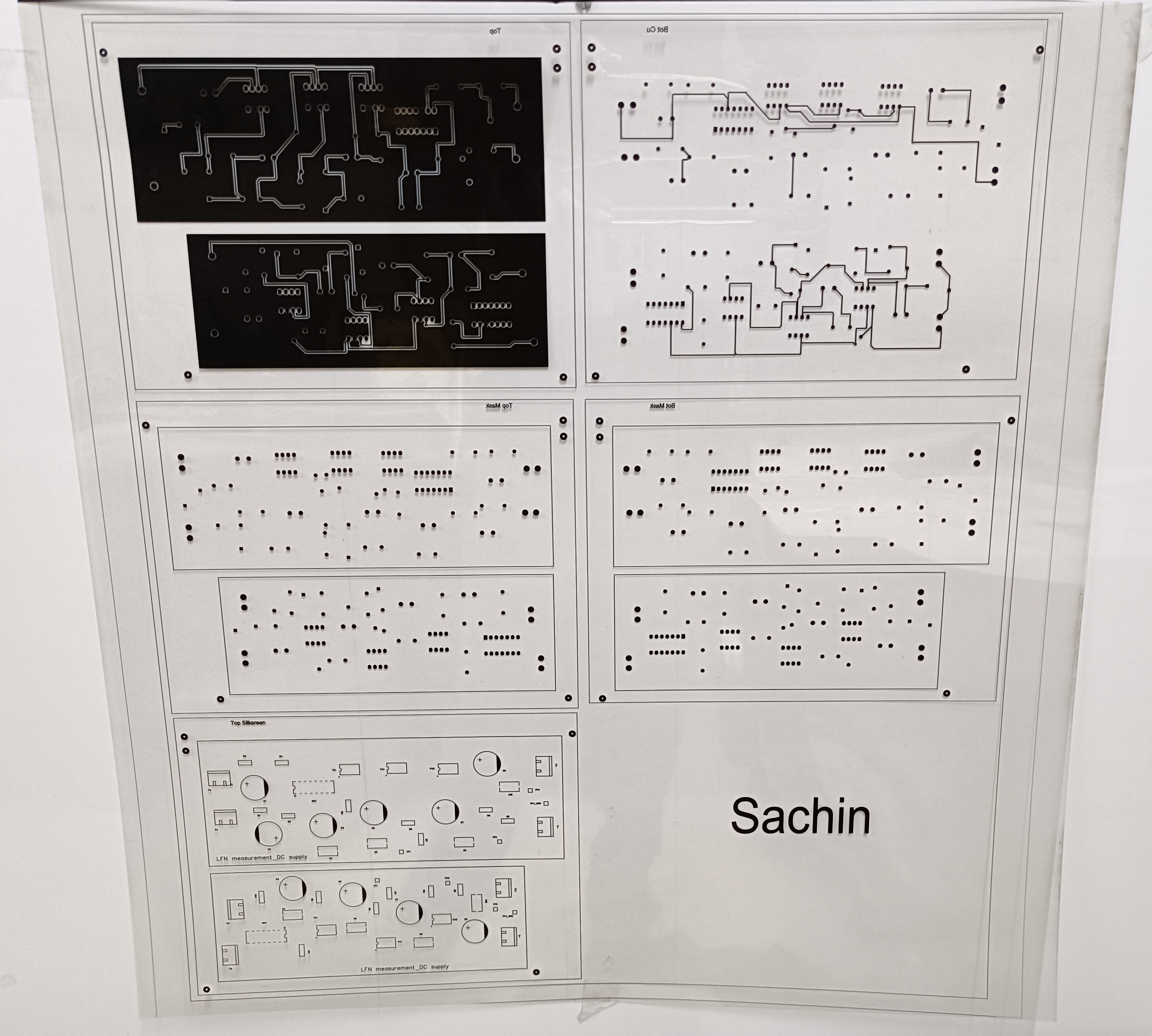
    In printed circuit board (PCB) fabrication, photofilm is used as a mask for photoresist layers. The design of the PCB, including traces and pads, is printed onto the photofilm, which is then placed over the photoresist layer on a PCB board. When exposed to UV light, the image on the photofilm transfers onto the photoresist, creating a pattern for etching.

    Prof. Laxmeesha Somappa

    In Charge, PCB LAB

    View Details

    Mr. Yadnik Sonalkar

    Technical Superintendent

    Ms. Manisha Bansode

    Junior Mechanic

  • Address : PCB LAB (Room No: 116-A, 1st Floor), Electrical Annex Building, Electrical Engineering Department, IIT Bombay, Powai, Mumbai, Maharashtra 400076.
  • Phone : +91-22-2159-3599
  • Email : pcblab@ee.iitb.ac.in