Germanium has emerged as a candidate for future CMOS technologies due to higher carrier mobilities than Si and its compatibility with Si manufacturing processes. However significant fundamental and technological challenges still remain in realising high quality gate stacks, low resistance contacts and source-drain junctions with high dopant concentration and low leakage. Our research group has been working on all these aspects of Ge transistors.
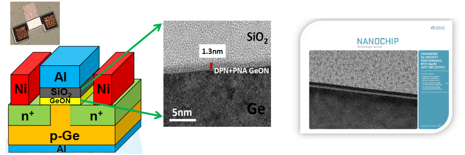
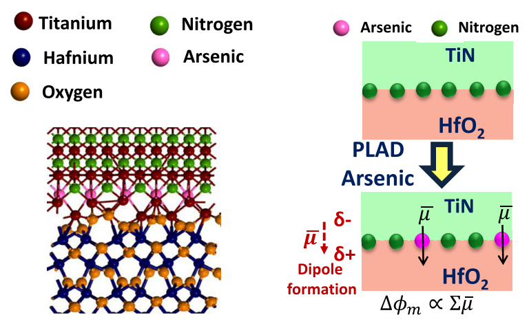
Gate Stacks:Ge gate stack with GeON interlayer dielectric [1]Our work has focussed on thermal stability of the high-k and gate interlayer (IL) dielectric layers, work-function tuning of n and p-FET gate stacks for multi-VT transistors, and reliability of scaled gate stacks. In some of our early work we showed that decoupled plasma nitridation of the GeO2 interlayer to form a GeON interlayer results in improved thermal stability without compromising significantly on carrier mobility [1]. Later we showed that HfO2 high-k layers can be alloyed with Al to form thermally stable HfAlO/GeO2 gate stacks on Ge channels. More recently we have shown, in collaboration with Applied Materials, controlled tuning of the effective work function in Ge gate stacks using nitrogen and arsenic plasma assisted doping for Ge p- and n-FinFET applications respectively [2]. Ultra-fast PBTI reliability measurements on scaled 1 nm stacks shown that trap generation at the high-k/IL interface is the key degradation mechanism [3].
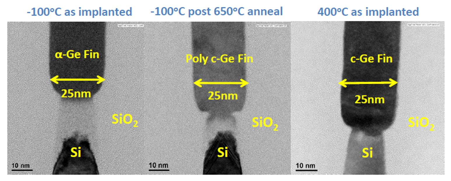
Source-drain Junctions:Cryogenic and hot implants in Ge fins
Using cryogenic implantation of P and B we have demonstrated significant n+ and p+ doping enhancement in Ge along with reduced leakage and/or improved on-current in n+/p and p+/n junction diodes respectively [4]. However, hot implants seem to be the way to go for fin implants where one needs to ensure an un-amorphized fin is available for junction regrowth.
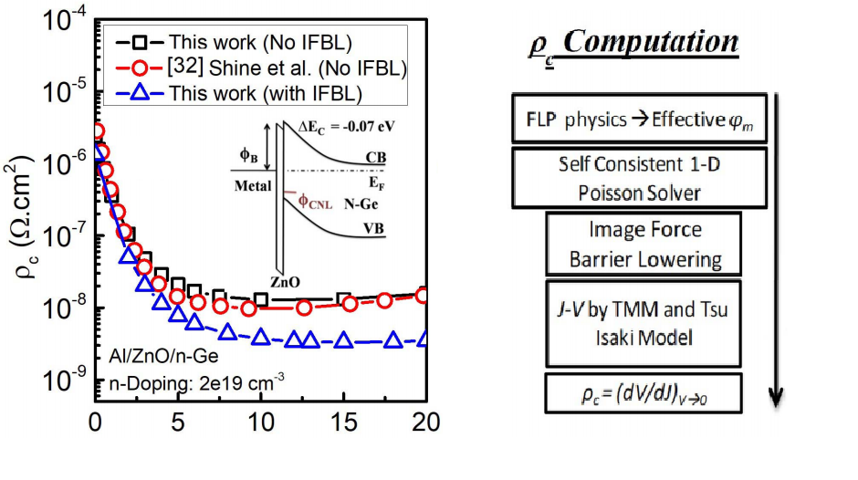
Source-drain Contacts: Fermi-level pinning near the valence band along with low phosphorus dopant activation makes the problem of high contact resistance to n-Ge particularly severe. In one of our first works on we demonstrated a novel metal-doped interfacial layer (ZnO)-Ge (MIS) contact scheme that helps alleviate Fermi-level pinning and at the same time reducesseries resistance through doping of ZnO [5]. Later we showed that this scheme can be leveraged to reduce contact barrier height further through the use of aMIS contacts on n-Ge using ZnO [6] and TiO2 interlayers [7]low work-function metal (Yb) [6]. More recently we have shown that the thermal stability of MIS contacts can be enhanced by nitridation of the interfacial layer without compromising on contact resistance [7].
We have recently shifted our focus towards GeSn for gate stacks and contacts. As a first step we have been able to grow high quality, crystalline GeSn layers on Ge substrates using sputtering and SPE. As is evident from the wide variety of experiments mentioned above, our group offers an excellent opportunity to think, design and execute new ideas related to device design and fabrication as well as process development for advanced CMOS applications.
Key publications:
P. Bhatt et al., “Germanium oxynitride gate interlayer dielectric formed on Ge(100) using decoupled plasma nitridation”, Applied Physics Letters, 103, 172107 (2013). Link
S. Kothari et al.,”Metal Gate VT Modulation Using PLAD N2 Implants for Ge P-FinFET Applications”, ESSDERC, Austria, (2015). Link “Plasma-assisted As Implants For Effective Work Function Modulation of TiN/HfO2 Gate Stacks on Germanium”, Applied Physics Letters, 112 (20), 203503 (2018). Link
C. Joishi et al., “Ultrafast PBTI characterization on Si-free gate last Ge nFETs with stable and ultrathin Al2O3 IL” International Reliability Physics Symposium (IRPS), Monterey, CA, April 2017. Link
“Understanding PBTI in replacement metal gate Ge n-channel FETs with ultrathin Al2O3and GeOx ILs using ultrafast charge trap-detrap techniques”, IEEE Transactions on Electron Devices, 65 (10), 4245-4253 (2018). Link
P. Bhatt et al., “High Performance 400 ºC p+/n Ge Junctions Using Cryogenic Boron Implantation”, IEEE Electron Device Letters, 35 (7), 717-719 (2014). Link
P. Paramahans et al.,“ZnO: an attractive option for n-type metal-interfacial layer-semiconductor (Si, Ge, SiC) contacts”, VLSI Symposium on Technology, Hawaii, June 12-15 (2012). “Fermi-level unpinning and low resistivity in contacts to n-type Ge with a thin ZnO interfacial layer”, Applied Physics Letters, 101, 182105 (2012). Link
S. Dev et al.,“Low resistivity contact on n-type Ge using low work-function Yb with a thin TiO2 interfacial layer”, Applied Physics Letters, 108 (10), 103507 (2016). Link
D. Biswas et al.,“Enhanced thermal stability of Ti/TiO2/n-Ge contacts through plasma nitridation of TiO2 interfacial layer”, Applied Physics Letters, 110, 052104 (2017). Link
(B) Modeling and Simulation:
Ab-initio DFT calculations of TiN/HfO2 interfaceMIS contact resistivity simulations [2]
Our efforts in device modeling and simulation foradvanced CMOS devices can be broadly classified into two categories. Firstly, we have developed an MIS contact simulator using a self-consistent SP solution with image force lowering and Fermi-level unpinning physics to compute the contact resistivity and effective barrier height of MIS contacts. Using this simulator we have shown the impact of IL doping on contact resistivity [1] as well as the impact of metal work-function variation on variability in contact resistivity [2]. Our current efforts are aimed at incorporating the effect of source/drain random dopant and IL thickness variation in this simulator to build a comprehensive picture of MIS and MS contact resistivity variability at advanced CMOS nodes.
Secondly, in collaboration with Prof. Swaroop Ganguly, we have carried out atomistic studies of the TiN/HfO2 gate metal/dielectric interface to understand the effective work function modulation observed in As-implanted gate stacks.
Key publications:
S. Gupta et al., “Contact resistivity reduction through interfacial layer doping in metal-interfacial layer-semiconductor contacts”, Journal of Applied Physics, 113, 234505 (2013). Link
S. Dev, M. Meena, Harshvardhan, S. Lodha, “Statistical Simulation Study of Metal Grain Orientation Induced MS and MIS Contact Resistivity Variability for 7 nm FinFETs”, IEEE Transactions on Electron Devices, 65 (8), 3104-3111 (2018). Link