Prof. Saurabh Lodha
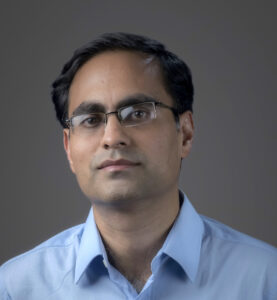 Prof. Saurabh Lodha is P. K. Kelkar Chair Professor at the Department of Electrical Engineering, Indian Institute of Technology (IIT) Bombay. He graduated from IIT Bombay in 1999 with a B. Tech (EE), followed by a Masters (ECE) and PhD (ECE) from Purdue University, USA, in 2001 and 2004, respectively. From 2005-2010 he worked at Intel Corporation in Portland, USA, on the research and development of 45, 32 and 22 nm Si CMOS technologies. He joined IIT Bombay in 2010, where he is also the Professor-in-charge of the IITB-OSU Frontier Research Center. His research interests span devices and materials in the areas of advanced CMOS technologies, 2D (opto)electronics and gallium oxide power electronics. He has been awarded the Swarna Jayanti fellowship (2017) and the Young Career Award (2020) by the Department of Science and Technology, Govt. of India. He has (co-)authored 102 peer-reviewed journal publications and 10 patents; his work has been cited more than 6000 times (h-index of 38). He is a fellow of INAE, a senior member of IEEE and has supervised 20 PhD students and 9 Postdocs.
CV (July 2023) – Personal Webpage – Google Scholar
Post Doctoral Fellows
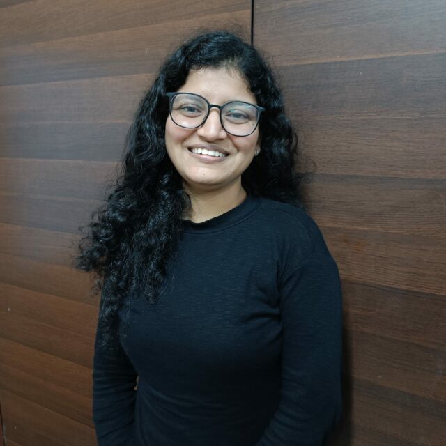

Dr. Mamta Raturi
Research Area:
2D Materials and Devices
Bio:
Mamta pursued her B.Sc. (General) from Panjab University, Chandigarh, and her M.Sc. in Physics from Punjabi University, Patiala. She worked as a JRF at IISER Mohali and completed her PhD from the Institute of Nano Science and Technology, Mohali, in 2023.
Research Interests:
Her research interest focuses on 2D optoelectronic devices.
Dr. Shivaram Kubakaddi
Dr. Raju Naik
PhD Scholars
-
Srilagna Sahoo
-
Prabhat Prajapati
-
Atira Zahoor
-
Subham Mahanti
-
Mayank Goyal

-
Mansi Patil
-
Shreyasi Das

-
Sera Sen
-
Kalpita Das

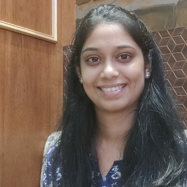
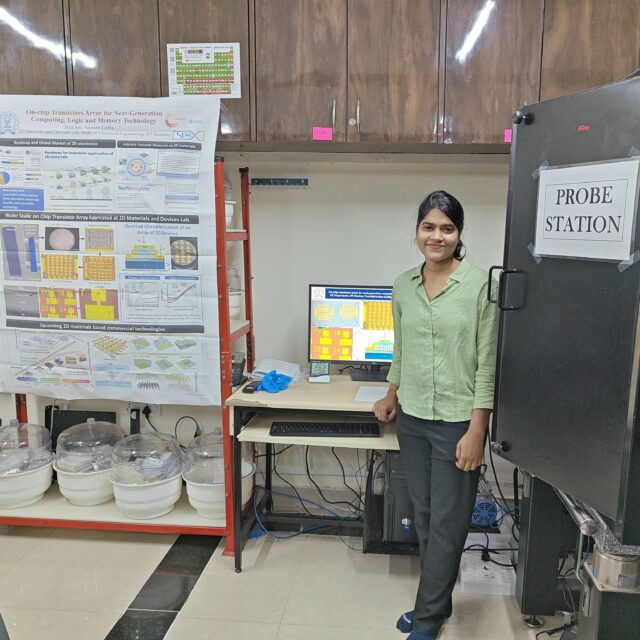
Srilagna Sahoo
Research Area:
2D Materials and Devices
Bio:
Srilagna has pursued her B.Tech. in Electronics and Telecommunication from BPUT, Odisha and M.Tech in VLSI and Microsystems from IIST, Trivandrum. She joined the Electrical Engineering department, at IIT Bombay, in Jan 2020 as a PhD student.
Research Interests:
Her research work in the lab focuses on the fabrication of 2D ferroelectric material transistors for memory applications.
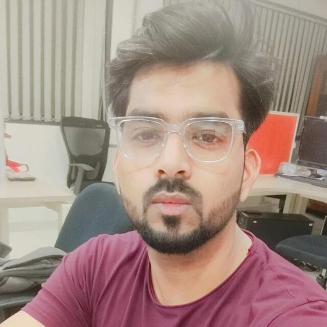
Prabhat Prajapati
Research Area:
Power Devices
Bio:
Since 2020, Prabhat, a skilled researcher, has worked to advance wide-bandgap semiconductor power devices at the Indian Institute of Bombay’s Electrical Engineering Department. He has an impressive academic background and was awarded a gold medal in 2018 for his outstanding work in the field of electronics at the University of Delhi’s post-graduate level. Prior to this, Prabhat held the distinction of being the top student in his Physical Science undergraduate program at Hindu College, University of Delhi, in 2015.
Research Interests:
His research focuses on wide-bandgap semiconductor materials like gallium oxide for the fabrication and characterization of power devices.
Atira Zahoor
Research Area:
2D Materials and Devices
Bio:
Research Interests:
Subham Mahanti
Research Area:
2D Materials and Devices
Bio:
Subham Mahanti completed his B.Sc. in Physics from the University of Calcutta in 2019, followed by an M.Sc. in Physics from the University of Delhi in 2021. He specialized in condensed matter physics and nanoscale physics. In 2022, Subham worked briefly as an Academic Specialist at Byju’s. Later that year, in July 2022, he joined the Centre for Research in Nanotechnology and Sciences (CRNTS) at IIT Bombay as a PhD student.
Research Interests:
2D material-based optoelectronics, Quantum Technologies
Mayank Goyal
Research Area:
2D Materials and Devices
Bio:
Mayank Goyal completed his BS-MS dual degree course from the Indian Institute of Science Education and Research (IISER) Pune in 2020 with a specialisation in Physics. He has done research internships at the University of Michigan, Ann Arbor, USA and INSP, Sorbonne University, Paris, France, which resulted in 4 co-authorships and 2 acknowledgements in reputed journal publications. He joined the PhD program in the Department of Electrical Engineering, IIT Bombay, through the Visvesvaraya PhD Scheme for Electronics & IT and later converted to the Prime Minister’s Research Fellowship.
Research Interests:
Layered 2D material-based optoelectronic devices
Mansi Patil
Research Area:
Advanced CMOS Devices
Bio:
Mansi Patil completed her BS-MS dual degree course from the Indian Institute of Science Education and Research (IISER) Bhopal in June 2023 with a specialization in Electrical Engineering and Computer Science (EECS). In July 2023, she joined PhD in Solid State Devices in the Electrical Engineering Department at IIT Bombay.
Research Interests:
Design, fabrication and characterization of amorphous oxide semiconductor-based thin-film transistors focusing on the back end of the line applications
Shreyasi Das
Research Area:
2D Materials and Devices
Bio:
Shreyasi Das is a graduate of the Institute of Radio Physics and Electronics, University of Calcutta, and is currently pursuing research on 2D materials and devices at IIT Bombay. Her research journey began with the IASc-NASI-INSA Summer Research Fellowship Program, where she worked on TCAD-based assessment of AlGaN/GaN HEMTs, resulting in multiple conferences and reputed journal publications. Her B.Tech dissertation, MEMS for biomedical applications, focused on developing novel silicon hollow microneedles for painless drug delivery. For her Master’s thesis, she worked towards ZnO nanowire and thin film-based MEMS sensors for biomedical applications. She also explored on-body RF sensors, which has resulted in a journal publication. She has served as a teaching assistant at IIT Bombay.
Research Interests:
Straintronics in few-layer Transition Metal Dichalcogenide (TMDs) devices to enhance transistor and optoelectronic performance
Sera Sen
Research Area:
2D Materials and Devices
Bio:
Sera Sen completed her B.Sc. (Hons) and M.Sc. in Electronics Science from Rajabazar Science College, University of Calcutta, in 2018 and 2020, respectively. She worked as a Project Research Associate in the Department of Electrical Engineering at IIT Bombay before joining the PhD program in January 2024.
Research Interests:
- Wafer-scale growth of 2D materials using ALD(Atomic Layer Deposition) and CVD(Chemical Vapor Deposition) tools, followed by characterization of those wafer-scale grown materials.
- Development of process flow for transistor fabrication on ALD and CVD grown 2D materials for electrical and neuromorphic applications.
Kalpita Das
Masters Students
Devarshi Dhoble
Tanishq Kale
Research Staff
