Ga2O3 is a promising material for power devices due to its ultra-wide bandgap (4.8-4.9 eV), enabling high breakdown voltage and efficient operation at high power densities. Its excellent electric field strength and potential for low-cost bulk crystal growth make it ideal for next-generation power electronics. Our work focuses on developing devices such as Schottky diodes [3, 4, 5, 6, 7], heterostructures and MOSFETs [8]. We have also demonstrated performance enhancement by incorporating advanced gate stacks [1, 2].
Key publications:-
- D. Biswas et al., “Enhanced n-type β-Ga2O3 (2¯01) gate stack performance using Al2O3/SiO2 bi-layer dielectric”, Applied Physics Letters, 114, 212106 (2019). Link
- D. Biswas et al., “Charge trap layer enabled positive tunable Vfb in β-Ga2O3 gate stacks for enhancement mode transistors”, Applied Physics Letters, 117, 172101 (2020). Link
- P Tiwari et al., “Nb2O5 high-k dielectric enabled electric field engineering of β-Ga2O3 metal-insulator-semiconductor (MIS) diode”, Journal of Applied Physics, 130 (24), 245701 (2021). Link
- R. Lengare et al., “Electrostatic Engineering of β-Ga2O3 Trench MIS Schottky Barrier Diodes Using a Bilayer Dielectric Stack”, IEEE Transactions of Electron Devices, 69 (10), 5476-5483 (2022). Link
- P. Sharma et al., “β-Ga2O3 Schottky Barrier Height Improvement Using Ar/O2 Plasma and HF Surface Treatments”, Applied Physics Letters, 124 (7), 072106 (2024). Link
- P. Prajapati et al., “Barrier height enhancement in β-Ga2O3 Schottky diodes using an oxygen-rich ultra-thin AlOx interfacial layer”, Applied Physics Letters, 125 (6), 061602 (2024). Link
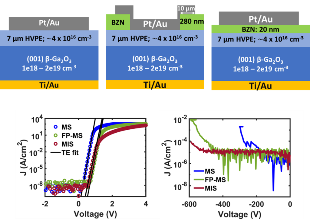
- P. Sharma et al., “Electric field management in β-Ga2O3 vertical Schottky diodes using high-k bismuth zinc niobium oxide”, Applied Physics Letters, 125 (24), 242105 (2024). Link
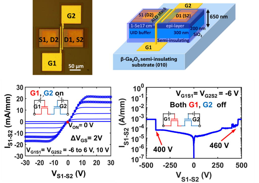
- P. Sharma et al., “Monolithic β-Ga2O3 Bidirectional Dual-Gate MOSFET”, Applied Physics Letters, 125 (25), 253502 (2024). Link