IIT BOMBAY
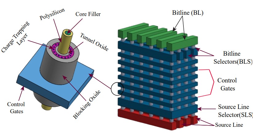
NAND flash memory is widely favored in storage systems for its high data density, cost-effectiveness, and fast read/write performance,
making it an ideal solution for modern devices such as smartphones, SSDs, and data centers. Its vertical stacking architecture,
used primarily in 3D NAND technology, has revolutionized storage by increasing density without increasing the physical footprint.
However, this advancement comes with significant data security challenges that demand attention.
The vertical stacking of memory cells can introduce greater complexity in terms of data management, making it harder to isolate and protect data.
My research focuses on addressing these security and reliability issues by characterizing various commercially available NAND flash memory chips in
different operational environments. By closely monitoring cell behavior, particularly in terms of bit flipping and BER, I aim to identify
the conditions under which NAND flash memory is most vulnerable to data corruption. This involves conducting extensive testing in
temperature-controlled environments, as well as simulating real-world usage patterns to observe how the chips behave under stress.
3D NAND Flash Memory has great potential for neuromorphic computing, a field in artificial intelligence inspired by the brain's efficiency in processing and storing information. Its vertical stacking enables high-density data storage, making it ideal for mimicking synapses in AI systems. Its non-volatile nature retains synaptic weights without power, allowing low-power, efficient computation. This technology could enhance the performance of AI in robotics and cognitive computing. However, challenges like endurance limits, speed, and analog precision must be overcome for scalable, brain-inspired architectures.
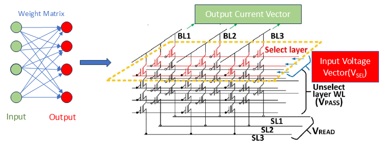
In-memory computing using Resistive Random-Access Memory (RRAM) is a cutting-edge approach aimed at overcoming
the limitations of traditional computing architectures. RRAM stores data by altering the resistance of its memory cells,
enabling non-volatile data retention and high-density storage. In an in-memory computing paradigm, data is processed
directly within the memory arrays, significantly reducing the latency and energy consumption associated with data movement between the memory
and the CPU. RRAM’s fast switching speed, scalability, and low power consumption make it a promising candidate for neuromorphic computing,
artificial intelligence, and edge computing applications.
Our research extends from single RRAM devices to dense RRAM Crossbar Array integration with FPGA based control circuitry exploiting MAC
operations for various AI algorithms improving computing efficiency.
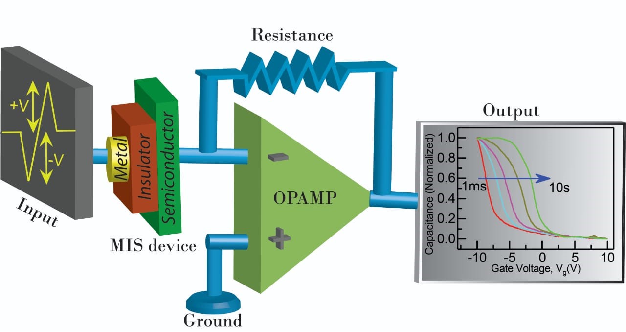
We are developing a high-speed current-voltage (CV) measurement system for metal-oxide-semiconductor (MOS) devices
that employs rapid voltage ramps to extract large-signal CV characteristics. This method allows for efficient and precise characterization of electrical properties,
providing critical data on flatband voltage, device capacitance and other parameters.
Our system also features programming and erasing capabilities for memory devices,
essential for evaluating the reliability of non-volatile memory technologies.
These fast cycles enhance testing throughput, facilitating quicker iterations in device development.
Overall, this tool aims to advance research in semiconductor technologies,
optimizing MOS devices and memory solutions. By delivering accurate measurements and valuable insights,
it will significantly contribute to the field.
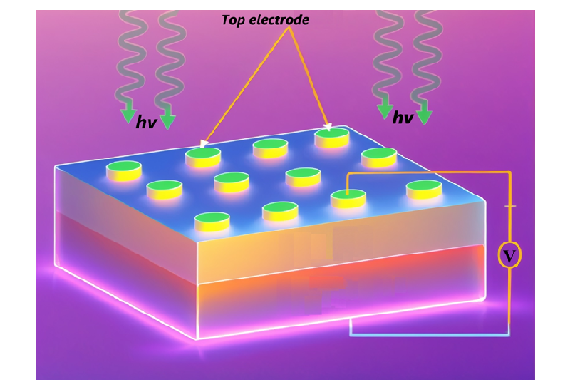
This research focuses on the impact of light on the electrical and optical properties of transparent memory devices. Transparent memory devices, designed with oxide semiconductors and transparent electrodes, offer potential for next-generation optoelectronic applications. Initially, we are focused on studying the light illumination effect on the Metal-Oxide-Semiconductor (MOS) structures. This study investigates how light illumination influences capacitance-voltage (C-V) characteristics, shifting inversion regions, and modulating interface trap densities. By analyzing these effects, the work aims to enhance the understanding of light-induced charge trapping, switching behavior, and overall device performance, contributing to advancements in transparent, light-responsive memory technologies. Our main goal is to fabricate light erasable memory devices on some flexible substrate.
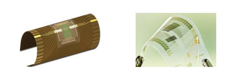
My research lies in the fascinating field of fabrication and characterization of Flexible NAND flash memories for flexible electronics applications. As the demand for portable and wearable electronic devices continues to grow, the development of flexible memory solutions becomes increasingly essential. NAND flash memories are renowned for their non-volatile nature and high data storage capabilities, making them ideal candidates for flexible electronics. My focus is on exploring innovative fabrication techniques that enable the integration of NAND flash memories into flexible substrates, such as PET(Polyethylene terephthalate) and Polyethylene Naphthalate (PEN) without compromising their performance and reliability. Additionally, I am intrigued by the challenges posed by characterizing the electrical and mechanical properties of these flexible memories, as this crucial aspect ensures their long-term functionality and resilience under various bending and stretching conditions. Through this research, I aim to contribute to the advancement of flexible electronics, unlocking new possibilities for applications in wearable devices, flexible displays, and beyond.
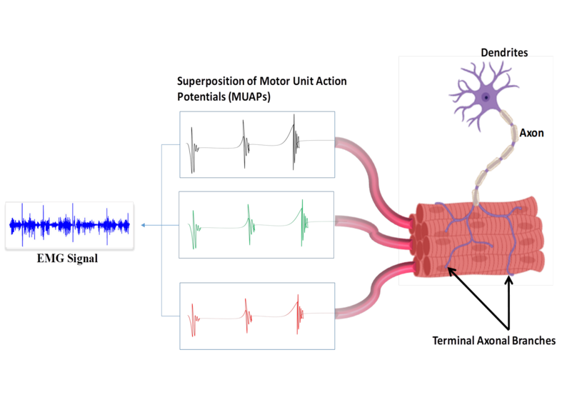
In sophisticated neurological surgeries, surgical incisions are made in close proximity to critical
areas such as the brainstem, spinal cord, cortex, and neuromuscular junctions. Unfortunately,
there is a significant risk of nerve injury during these procedures. To address this challenge,
surgeons employ a technique called Intraoperative Neurological Monitoring (IONM). The real-
time monitoring provided by IONM enables surgeons to assess potential nerve damage and make
necessary adjustments during the surgery to optimize patient outcomes.
Our group is working on an exceptionally versatile and elegant Fan-Out Wafer-Level Packaging
(FOWLP) based fully integrated bipolar multi-channel surface electromyography (sEMG)
device. This innovative device is designed specifically for intraoperative neurological monitoring
(IONM) during complex spine surgeries, as well as for post-operative physiological monitoring.