
CV Measurement Fundamentals
Why do engineers make so many mistakes when measuring capacitance (especially on-wafer)?
The most common reasons are :- Capacitance measurement requires compensation to remove parasitic inductance and capacitance from the measurement cables and fixturing, and many times this is done improperly (or not at all).
- An induced current flows through the outer shield of BNC, connectors (if used) on a capacitance meter, and this current is necessary to balance the measurement current of the capacitance meter. If the outer shield is grounded, then the induced current flow is shorted to ground and the bridge may not be able to balance. Many users are unaware of this issue.
- Measuring capacitance on a semiconductor wafer on a wafer chuck is very different from measuring a discrete device. The effects of the wafer prober chuck on the measurement cannot be ignored.
- For higher measurement frequency (>5MHz), structure (layout) design has a major impact on the success or failure of the measurements.
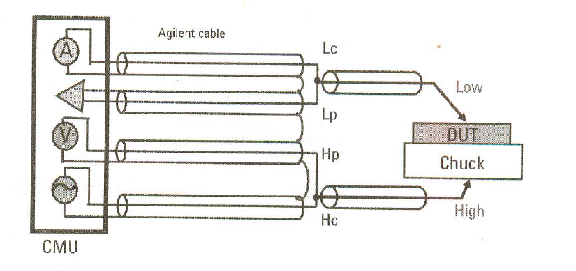
The 4TP measurement method
The most common measurement technique used with the auto balancing bridge capacitance meter is the 4 terminal measurements. In this procedure the Hc and Hp terminal and the Lc and Lp terminal are shorted together as shown in the figure below.
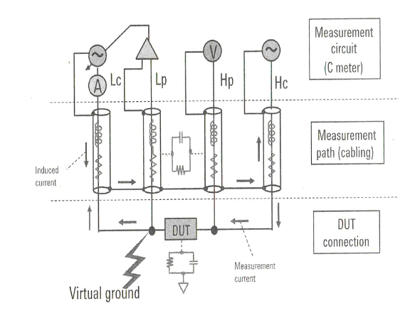
The Hp and Hc terminal are commonly referred to as the CMH (capacitance meter high) connection and the Lp and Lc terminals are commonly referred to as the CML (capacitance meter low) connection. These is residual inductance and resistance in the measurement path (cabling) and stray capacitance both between the cables and between the DUT and ground (which are also shown in the previous figure).The user must perform compensation through the measurement path in order to eliminate the effects of these parasitic element or the accuracy of the measurement will be seriously degraded.
The CML terminal of the 4TP scheme is a virtual ground and it is very important NOT to tie this point to earth ground. If the CML terminal contacts earth ground then the auto balancing bridge circuit will not be able to balance and you will get measurement errors. The outer conductor (shield) of the capacitance cables has the same potential as the virtual ground, and it needs to be floated as well. In addition, the four outer shields should be connected together just before the probe tips with cables that are short in length. This creates a return path for the current that is induced in the shield, which stabilizes the series inductance of the cables. Unless the outer shields are shorted and the series inductance stabilized, the mere act of changing the cable separation will cause large variations in cable inductance that immediately invalidate any cable compensation that has been performed.
The Importance of Proper Compensation
For capacitance meters, the "calibration plane" defines the point (normally the BNC outputs of the capacitance meter) at which the user can obtain the specified measurement accuracy of the capacitance meter. Of course, for parametric test we need to use cabling to test our DUT.In the case of the 4TP measurement method this introduces a variety of sources of error due to residual parasitic elements in the test fixturing (cables).
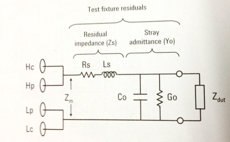
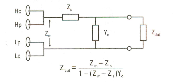
To remove the effect of these test fixture residuals, we perform two measurements: one with test terminals open and one with the test terminals shorted as shown below.
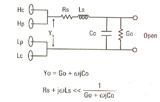
Using these two values, we can calculate the true value of Zdut from the measured value (Zm) using the equation shown below.
ON Wafer Capacitance Measurement
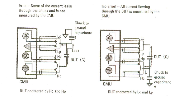
There are some important issues to take into account when making on wafer capacitance measurements. The most importance of these is how the Hc and Hp and Lc and Lp terminals contact the wafer. Many people know from experience that they get much better measurement results by contacting the Lc and Lp terminal to the wafer (DUT) and contacting the Hc and Hp terminal to the wafer chuck when using the 4TP cabling method.
However, most people do not know why this provides better measurement results. The reason that you obtain better measurement results using this technique can be understood by remembering that on a wafer prober you have to be concerned with chuck-to-ground capacitance. When making measurement at frequency, the chuck capacitance acts as a sneak path to ground. Consider the two different cases shown below.
Making capacitance measurements through a switching matrix
One long-running issue in parametric test has been called "the CV-IV measurement dilemma". The dilemma referred to has to do with the different cabling needs of capacitance meters and SMUs. Capacitance meters use BNC cables and SMUs use triaxial cables, yet most parametric testing requires both CV and IV measurements. Manually switching from triaxial to BNC cables (and back again) is extremely tedious and it also does not permit any sort of test automation. Obviously, switching matrices represent one solution to this problem. In this section we will discuss the proper way to make capacitance.
Switching matrix capacitance measurement issues
Most of the errors that occur when making capacitance measurement through a switching matrix can be attributed to one or more of the following factors:
- Non –standard CMU cables or an unsupported cables length are used to connect the capacitance meter to the switching matrix.
- The guards are not shorted together close to the DUT.
- The cable extensions create cable impedance mismatch.
- The matrix does not support any sort of compensation scheme(opening/closing of input-to-output connections)
Parametric Measurement Hand Book, First Edition, Agilent Technologies
← Back to Resources