Electrical Engineering

Indian Institute of Technology Bombay

People

People

Faculty

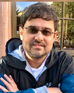
Souvik Mahapatra
Qualifications

• MSc (Physics), Jadavpur University, Calcutta, 1995
• PhD (Electrical Engineering), IIT Bombay, 1999

Research Interests

• Electrical characterization, modeling and simulation of micro/nano electronic devices
• NBTI/PBTI and Hot carrier degradation in MOSFETs
• High-k gate dielectrics
• Advanced CMOS device reliability
• Flash EEPROMs – Floating gate, SONOS/SANOS & Metal Nanopartic

Work Experience

• PMTS, Bell Laboratories, Lucent Technologies, Murray Hill, NJ, USA (2000 – 2001)
• Assistant Professor, Department of Electrical Engineering, IIT Bombay (2002 – 2004)
• Associate Professor, Department of Electrical Engineering, IIT Bombay (2005 – 2008)

Journal Papers


  1. Narendra Parihar, Richard G. Southwick, Miaomiao Wang, James H. Stathis, and Souvik Mahapatra, "Modeling of NBTI Kinetics in RMG Si and SiGe FinFETs, Part-I: DC Stress and Recovery", IEEE Transactions on Electron Devices, vol. 65, pp. 1699-1706, May 2018. [DOI]
  2. Narendra Parihar, Nilesh Goel, Subhadeep Mukhopadhyay, and Souvik Mahapatra, "BTI Analysis Tool—Modeling of NBTI DC, AC Stress and Recovery Time Kinetics, Nitrogen Impact, and EOL Estimation", IEEE Transactions on Electron Devices, vol. 65, pp. 392-403, Feb. 2018. [DOI]
  3. Narendra Parihar, Uma Sharma, Richard G. Southwick, Miaomiao Wang, James H. Stathis, and Souvik Mahapatra, "Ultrafast Measurements and Physical Modeling of NBTI Stress and Recovery in RMG FinFETs Under Diverse DC–AC Experimental Conditions", IEEE Transactions on Electron Devices, vol. 65, pp. 23-30, Jan. 2018. [DOI]
  4. N. Parihar, R. Southwick, M. Wang, J. H. Stathis, and S. Mahapatra, "Modeling of NBTI time kinetics and T dependence of VAF in SiGe p-FinFETs", 2017 IEEE International Electron Devices Meeting (IEDM), Dec. 2017. [DOI]
  5. Narendra Parihar, Nilesh Goel, Ankush Chaudhary, and Souvik Mahapatra, "A Modeling Framework for NBTI Degradation Under Dynamic Voltage and Frequency Scaling", IEEE Transactions on Electron Devices, vol. 63, pp. 946-953, Mar. 2016. [DOI]
  6. P. K. Singh, G, Bisht, K. Auluck, M. Shivatheja, R. Hofmann, K. K. Singh, and S. Mahapatra, "Performance and reliability study of single layer and dual layer Platinum nanocrystal Flash memory devices under NAND operation", to appear, IEEE Trans. Electron Devices, 2010.
  7. C. Sandhya, A. B. Oak, N. Chattar, U. Ganguly, C. Olsen, S. M. Seutter, L. Date, R. Hung, J. Vasi, and S. Mahapatra, "Study of P/E cycling endurance induced degradation in SANOS memories under NAND (FN/FN) operation", IEEE Trans. Electron Devices, vol. 57, pp. 1548, 2010.
  8. A. Datta and S. Mahapatra, "A comprehensive analysis on scaling prospects of dual-bit channel engineered SONOS NOR-flash EEPROM cells", Solid State Electron, vol. 54, pp. 397, 2010.
  9. S. Mahapatra, V. D. Maheta, A. E. Islam, and M. Alam, "Isolation of NBTI stress generated interface trap and hole trapping components in PNO p -MOSFETs", IEEE Trans. Electron Devices, vol. 56, pp. 236, 2009.
  10. S. Deora, V. D. Maheta, G. Bersuker, C. Olsen, K. Ahmed, R. Jammy, and S. Mahapatra, "A comparative NBTI study of HfO2, HfSiOX and SiON p-MOSFETs using UF-OTF IDLIN technique", IEEE Electron Dev. Lett, vol. 30, pp. 152, 2009.
  11. S. Deora, A. E. Islam, M. A. Alam, and S. Mahapatra, "A common framework of NBTI generation and recovery in plasma nitrided SiON p-MOSFETs", IEEE Electron Dev. Lett, vol. 30, pp. 978, 2009.
  12. P. K. Singh, R. Hofmann, G. Bisht, K. K. Singh, N. Krishna, and S. Mahapatra, "Performance and reliability of Au and Pt single layer metal nanocrystal flash memory under NAND (FN/FN) operation", IEEE Trans. Electron Devices, vol. 56, pp. 2065, 2009.
  13. K. G. Anil, S. Mahapatra, and I. Eisele, "Electron-electron interaction signature peak in the substrate current vs gate voltage characteristics of n-channel silicon MOSFETs", IEEE Trans. Electron Devices, vol. 49, pp. 1283, 2009.
  14. C. Sandhya, U. Ganguly, N. Chattar, C. Olsen, S. M. Seutter, L. Date, R. Hung, J. Vasi, and S. Mahapatra, "Effect of SiN on performance and reliability of charge trap flash (CTF) under Fowler-Nordheim tunneling program/erase operation", IEEE Electron Dev. Lett, vol. 30, pp. 171, 2009.
  15. C. Sandhya, A. B. Oak, N. Chattar, A. S. Joshi, U. Ganguly, C. Olsen, S. M. Seutter, L. Date, R. Hung, J. Vasi, and S. Mahapatra, "Impact of SiN composition variation on SANOS memory performance and reliability under NAND (FN/FN) operation", IEEE Trans. Electron Devices, vol. 56, pp. 3123, 2009.
  16. A. Datta, R. Asnani, and S. Mahapatra,, "A novel gate assisted reverse read scheme to control bit coupling and read disturb for multibit/cell operation in deeply scaled split-gate SONOS flash EEPROM cells", IEEE Electron Dev. Lett, vol. 30, pp. 885, 2009.
  17. V. D. Maheta, E. N. Kumar, S. Purawat, C. Olsen, K. Ahmed, and S. Mahapatra, "Development of an ultra-fast on-the-fly IDLIN technique to study NBTI in plasma and thermal oxynitride p-MOSFETs", IEEE Trans. Electron Devices, vol. 55, pp. 2614, 2008.
  18. V. D. Maheta, C. Olsen, K. Ahmed, and S. Mahapatra., "The impact of nitrogen engineering in silicon oxynitride gate dielectric on negative bias temperature instability in p-MOSFETs: A study by ultra-fast on-the-fly IDLIN technique", IEEE Trans. Electron Devices, vol. 55, pp. 1630, 2008.
  19. P. K. Singh, G. Bisht, R. Hofmann, K. Singh, N. Krishna, and S. Mahapatra, "Metal nanocrystal memory with Pt single and dual layer NC with low leakage Al2O3 blocking dielectric", IEEE Electron Dev. Lett, vol. 29, pp. 1389, 2008.
  20. A. E. Islam, G. Gupta, K. Z. Ahmed, S. Mahapatra, and M. A. Alam, "Optimization of gate leakage and NBTI for plasma-nitrided gate oxides by numerical and analytical models", IEEE Trans. Electron Devices, vol. 55, pp. 1143, 2008.
  21. (Invited) S. Mahapatra and M. A. Alam, "Defect generation in p-MOSFETs under negative bias stress: An experimental perspective", IEEE Trans. Materials and Dev. Reliability, vol. 8, pp. 35, 2008.
  22. (Invited) A. E. Islam, H. Kufluoglu, D. Varghese, S. Mahapatra, and M. A. Alam, "Recent issues in negative bias temperature instability: Initial degradation, field dependence of interface trap generation, hole trapping effects and relaxation", IEEE Trans. Electron Devices, vol. 54, pp. 2143, Sep. 2007.
  23. D. Varghese, G. Gupta, L. Madhav, D. Saha, K. Ahmed, F. Nouri, and S. Mahapatra, "Physical Mechanism and Gate Insulator Material Dependence of Generation and Recovery of Negative Bias Temperature Instability in p-MOSFETs", IEEE Trans. Electron Devices, vol. 54, pp. 1672, Jul. 2007.
  24. P. Bharath Kumar, R. Sharma, P. R. Nair, and S. Mahapatra, "Investigation of drain disturb in SONOS Flash EEPROMs", IEEE Trans. Electron Devices, vol. 54, pp. 98, 2007.
  25. M. A. Alam, H. Kufluoglu, D. Varghese, and S. Mahapatra, "A Comprehensive Model of PMOS NBTI Degradation: Recent progress", Microelectronics Reliability, vol. 47, pp. 853, 2007.
  26. A. Datta, P. Bharath Kumar, and S. Mahapatra,, "Dual-bit/Cell SONOS Flash EEPROMs: Impact of Channel Engineering on Programming Speed and Bit Coupling Effect", IEEE Electron Dev. Lett, vol. 28, pp. 446, 2007.
  27. P. Bharath Kumar, P. R. Nair, R. Sharma, S. Kamohara, and S. Mahapatra, "Lateral profiling of trapped charge in SONOS Flash EEPROMs programmed using channel hot electron injection", IEEE Trans. Electron Devices, vol. 53, pp. 698, 2006.
  28. P. Bharath Kumar, D. Nair, and S. Mahapatra, "Using Soft Secondary Electron Programming to reduce Drain Disturb in Floating Gate NOR Flash EEPROMs", IEEE Trans. Device and Materials Reliability, vol. 6, pp. 81, 2006.
  29. D. Saha, D. Varghese, and S. Mahapatra, "The role of Anode Hole Injection and Valence Band Hole Tunneling on interface trap generation during hot carrier injection stress", IEEE Electron Devices Lett, pp. 585, 2006.
  30. D. Saha, D. Varghese, and S. Mahapatra, "On the Generation and Recovery of Hot Carrier Induced Interface Traps: A critical examination of the 2D Reaction Diffusion model", IEEE Electron Devices Lett, vol. 27, pp. 188, 2006.
  31. D. Varghese, S. Mahapatra, and M. A. Alam, "Hole energy dependent interface trap generation in MOSFET Si/SiO2 interface", IEEE Electron Devices Lett., vol. 26, pp. 572, Aug. 2005.
  32. D. R. Nair, S. Mahapatra, S. Shukuri, and J. Bude, "Explanation of P/E Cycling Impact on Drain Disturb in Flash EEPROMs under CHE and CHISEL Programming Operation", IEEE Trans. Electron Devices, vol. 52, pp. 534, 2005.
  33. (Invited) M. A. Alam and S. Mahapatra, "A Comprehensive Model of PMOS NBTI Degradation", Microelectronics Reliability, special issue on NBTI, vol. 45, pp. 71, 2005.
  34. S. Mahapatra, P. Bharath Kumar, and M. A. Alam, "Investigation and Modeling of Interface and Bulk Trap Generation During Negative Bias Temperature Instability of p-MOSFETs", IEEE Trans. Electron Devices, vol. 51, pp. 1371, 2004.
  35. D. R. Nair, S. Mahapatra, and S. Shukuri, "Cycling endurance of NOR Flash EEPROM cells under CHISEL programming operation - Impact of technological parameters and scaling", IEEE Trans. Electron Devices, vol. 51, pp. 1672, 2004.
  36. D. R. Nair, S. Mahapatra, S. Shukuri, and J. Bude, "Drain disturb during CHISEL programming of NOR Flash EEPROMs – Physical mechanisms and impact of technological parameters", IEEE Trans. Electron Devices, vol. 51, pp. 701, 2004.
  37. D. R. Nair, N. R. Mohapatra, S. Mahapatra, S. Shukuri, and J. Bude, "Effect of P/E cycling on drain disturb in Flash EEPROMs under CHE and CHISEL operation", IEEE Trans. Device and Materials Reliability, vol. 4, pp. 32, 2004.
  38. N. R. Mohapatra, D. R. Nair, S. Mahapatra, V. R. Rao, S. Shukuri, and J. Bude, "CHISEL programming operation of scaled NOR Flash EEPROMs – Effect of voltage scaling, device scaling and technological parameters", IEEE Trans. Electron Devices, vol. 50, pp. 2104, 2003.
  39. K. G. Anil, S. Mahapatra, and I. Eisele, "A detailed experimental investigation of impact ionization in n-channel metal-oxide-semiconductor field-effect-transistors at very low drain voltages”", Solid State Electron, vol. 47, pp. 997, 2003.
  40. S. Mahapatra, S. Shukuri, and J. Bude, "CHISEL flash EEPROM part-II: reliability", IEEE Trans. Electron Devices, vol. 49, pp. 1302, 2002.
  41. K. G. Anil, S. Mahapatra, and I. Eisele, "Experimental verification of the nature of the high energy tail in the electron energy distribution in n-channel MOSFETs", IEEE Electron Devices Lett, vol. 22, pp. 478, Oct. 2001.
  42. K. G. Anil, S. Mahapatra, and I. Eisele, "Observation of double peak in the substrate current versus gate voltage characteristics in n-channel MOSFETs", Appl. Phys. Lett, vol. 78, no. 15, pp. 2238, Apr. 2001.
  43. K. G. Anil, S. Mahapatra, V. R. Rao, and I. Eisele, "Comparison of sub-bandgap impact ionization in deep-submicron conventional and lateral asymmetric channel n-MOSFETs", Jpn. J. Appl. Phys, vol. 40, no. 4B, pp. 2621, Apr. 2001.
  44. S. Mahapatra, V. Ramgopal Rao, B. Cheng, M. Khare, C. D. Parikh, J. C. S. Woo and J. Vasi, "Performance and Hot-Carrier Reliability of 100 nm Channel Length Jet Vapor Deposited Si3N4 MNSFETs", IEEE Trans. on Electron Devices, vol. 48, pp. 679, 2001.
  45. S. Mahapatra, V. R. Rao, C. D. Parikh, J. Vasi, B. Cheng, and J. C. S. Woo, "A study of hot-carrier induced interface trap profiles in lateral asymmetric channel MOSFETs using a novel charge pumping technique", Solid State Electron, vol. 45, pp. 1717, 2001.
  46. S. Mahapatra, C. D. Parikh, V. Ramgopal Rao, C. R. Vishwanathan and J. Vasi, "A comprehensive study of hot-carrier induced interface and oxide trap distributions in MOSFETs using a novel charge pumping technique", IEEE Trans. Electron Devices, vol. 47, pp. 171, 2000.
  47. S. Mahapatra, V. R. Rao, C. D. Parikh, J. Vasi, B. Cheng, and J. C. S. Woo, "A study of 100 nm channel length asymmetric channel MOSFET by using charge pumping", Microelectronics Engineering, vol. 48, pp. 193, Sep. 1999.
  48. S. Mahapatra, C. D. Parikh, J. Vasi, V. R. Rao, and C. R. Viswanathan, "A direct charge pumping technique for spatial profiling of hot-carrier induced interface and oxide traps in MOSFETs", Solid State Electron, vol. 43, pp. 913, Jun. 1999.
  49. S. Mahapatra, C. D. Parikh, and J. Vasi, "A new ‘multifrequency’ charge pumping technique to profile hot-carrier induced interface-state density in n-MOSFETs", IEEE Trans. Electron Devices, vol. 46, pp. 960, May 1999.
  50. Mahapatra, C. D. Parikh and J. Vasi, "A new ‘multifrequency’ charge pumping technique to profile hot-carrier induced interface-state density in nMOSFETs", IEEE Trans. Electron Devices, vol. 46, pp. 960, 1999.

Conference Papers / Book Chapters

  1. S. Deora, V. D. Maheta, and S. Mahapatra, "NBTI lifetime prediction in SiON p-MOSFETs by H/H2 reaction diffusion (RD) and dispersive hole trapping model" in Proc., Int. Rel. Phys. Symp (IRPS), pp.1105, Dec. 2010.
  2. Z. Z. Lwin, K. L. Pey, Y. N. Chen, P. K. Singh, and S. Mahapatra, "Charging and discharging characteristics of metal nanocrystals in degraded dielectric stack" in Int. Rel. Phys. Symp, pp.981, Dec. 2010.
  3. P. Singh, C. Sandhya, K. Auluck, G. Bisht, M. Shivatheja, R. Hofmann, G. Mukhopadhyay, and S. Mahapatra, "Applicability of dual layer metal nanocrystal flash memory for NAND 2 or 3-bit/cell operation: Understanding the anomalous breakdown and optimization of P/E conditions" in in Proc., Int. Rel. Phys. Symp, pp.981, Dec. 2010.
  4. P. K. Singh, G. Bisht, M. Sivatheja, C. Sandhya, R. Hofmann, K. Singh, N. Krishna, G. Mukhopadhyay, and S. Mahapatra, "Reliability of SL and DL Pt NC devices for NAND Flash applications: A 2 region model for endurance defect generation" in in Proc., Int. Rel. Phys. Symp, pp.301, Dec. 2009.
  5. A. E. Islam, S. Mahapatra, S. Deora, V. D. Maheta, and M. A. Alam, "On the differences between ultra-fast NBTI measurements and reaction diffusion theory" in in Proc., IEEE Int. Elect. Dev. Meet. (IEDM), Dec. 2009.
  6. (Invited) S. Mahapatra and P. K. Singh, "Metal/high-k/metal nanocrystal gate stacks for NAND flash applications" in ECS meeting, Dec. 2009.
  7. (Invited) S. Mahapatra, V. D. Maheta, S. Deora, E. N. Kumar, S. Purawat, C. Olsen, K. Ahmed, A. E. Islam, and M. A. Alam, "Material dependence of negative bias temperature instability (NBTI) stress and recovery in SiON p-MOSFETs" in ECS meeting, Dec. 2009.
  8. (Invited) S. Mahapatra, V. D. Maheta, S. Deora, E. N. Kumar, S. Purawat, C. Olsen, K. Ahmed, A. E. Islam, and M. A. Alam, "Material dependence of negative bias temperature instability (NBTI) stress and recovery in SiON p-MOSFETs" in ECS meeting, Dec. 2009.
  9. P. K. Singh, G. Bisht, R. Hofmann, K. Singh, and S. Mahapatra, "Dual layer Pt metal NC Flash for MLC NAND application" in in Proc., Int. Memory Workshop, pp.78, Dec. 2009.
  10. Sandhya C, U. Ganguly, K.K. Singh, C. Olsen, S. M. Seutter, G. Conti, K. Ahmed, N. Krishna, J. Vasi, and S. Mahapatra, "The Effect of Band Gap Engineering of the Nitride Storage Node on Performance and Reliability of Charge Trap Flash" in Int. Phys. Failure Analysis conf, Dec. 2008.
  11. Sandhya C, U. Ganguly, K.K. Singh, P.K. Singh, C. Olsen, S. M. Seutter, R. Hung, G. Conti, K. Ahmed, N. Krishna, J. Vasi,, and S. Mahapatra, "Nitride engineering and the effect of interfaces on charge trap flash performance and reliability" in Int. Rel. Phys. Symp. (IRPS), Dec. 2008.
  12. Sandhya C., U. Ganguly, K.K. Singh, P.K. Singh, C. Olsen, S. M. Seutter, R. Hung, G. Conti, K. Ahmed, N. Krishna, J. Vasi and S. Mahapatra, "Nitride Engineering and the effect of interfaces on charge trap flash performance and reliability" in International Reliability Physics Symposium (IRPS), Dec. 2008.
  13. (Invited) S. Mahapatra and V. D. Maheta, "Gate insulator process dependent NBTI in SiON p-MOSFETs" in in Proc., Int. Conf. on Solid State and Integrated Circuit Technology (ICSICT), Dec. 2008.
  14. P. K. Singh, K. K. Singh, R. Hofmann, K. Armstrong, N. Krishna, and S. Mahapatra, "Au nanocrystal flash memory reliability and failure analysis" in Int. Phys. Failure Analysis conf, Dec. 2008.
  15. S. Deora and S. Mahapatra, "A study of NBTI in HfSiON/TiN p-MOSFETs using ultra-fast on-the-fly IDLIN technique" in Int. Phys. Failure Analysis conf., Dec. 2008.
  16. G. Kapila, N. Goyal, V. D. Maheta, C. Olsen, K. Ahmed, and S. Mahapatra, "A comprehensive study of flicker noise in plasma nitrided SiON p-MOSFETs: Process dependence of pre-existing and NBTI stress generated trap distribution profiles" in in Proc., IEEE Int. Elect. Dev. Meet. (IEDM), Dec. 2008.
  17. A. Nainani, S. Palit, P. K. Singh, U. Ganguly, N. Krishna, J. Vasi and S. Mahapatra, "Development of a 3D simulator for metal nanocrystal flash memories under NAND operation" in International Electron Devices Meeting (IEDM), Dec. 2007.
  18. A.E. Islam, E. N. Kumar, H. Das, S. Purawat, V. Maheta, H. Aono, E. Murakami, S. Mahapatra, and M.A. Alam, "Theory and Practice of Ultra-fast Measurements for NBTI Degradation: Challenges and Opportunities" in Int. Electron Dev. Meet. (IEDM), Dec. 2007.
  19. E. N. Kumar, V. D. Maheta, S. Purawat, A. E. Islam, C. Olsen, K. Ahmed, M. A. Alam, and S. Mahapatra, "Material Dependence of NBTI Physical Mechanism in Silicon Oxynitride (SiON) p-MOSFETs: A Comprehensive Study by Ultra-Fast On-The-Fly (UF-OTF) IDLIN Technique" in Int. Elect. Dev. Meet. (IEDM), Dec. 2007.
  20. A. Nainani, S. Palit, P. K. Singh, U. Ganguly, N. Krishna, J. Vasi, and S. Mahapatra, "Development of A 3D Simulator for Metal Nanocrystal (NC) Flash Memories under NAND Operation" in Int. Elect. Dev. Meet. (IEDM), Dec. 2007.
  21. S. Mahapatra, K. Ahmed, D. Varghese, A. E. Islam, G. Gupta, L. Madhav, D. Saha, and M. A. Alam, "On the Physical Mechanism of NBTI in Silicon Oxynitride p-MOSFETs: Can Differences in Insulator Processing Conditions Resolve the Interface Trap Generation versus Hole Trapping Controversy?" in in Proc., Int. Rel. Phys. Symp (IRPS), pp.1, Apr. 2007.
  22. A. E. Islam, G. Gupta, S. Mahapatra, A. T. Krishnan, K. Ahmed, F. Nouri, A. Oates, and M. A. Alam, "Gate leakage vs. NBTI in plasma nitrided oxides: Characterization, physical principles and optimization" in International Electron Devices Meeting (IEDM), pp.403, Dec. 2006.
  23. P. Bharath Kumar, E. Murakami, S. Kamohara,, and S. Mahapatra, "Endurance and Retention Characteristics of SONOS EEPROMs operated using BTBT Induced Hot Hole Erase" in Int. Reliability Phys. Symp (IRPS), Dec. 2006.
  24. A. Paul, Ch. Sridhar, S. Gedam, and S. Mahapatra, "Comprehensive simulation of program, erase and retention in charge trapping flash memories" in International Electron Devices Meeting (IEDM), pp.393, Dec. 2006.
  25. P. Bharath Kumar, D. R. Nair, and S. Mahapatra, "Soft Secondary Electron Programming for Floating Gate NOR Flash EEPROMs" in International Symposium on the Physical and Failure Analysis of Integrated Circuits, pp.146, Dec. 2005.
  26. Invited) S. Mahapatra, M. A. Alam, P. Bharath Kumar, T. R. Dalei, D. Varghese, and D. Saha, "Negative bias temperature instability in CMOS devices" in Microelectronics Engineering, special issue on INFOS, pp.114, Dec. 2005.
  27. P. Bharath Kumar, Ravinder Sharma, Pradeep R. Nair, Deleep R. Nair, S. Kamohara, S. Mahapatra, and J. Vasi, "Mechanism of drain disturb in SONOS Flash EEPROMs" in Int. Reliability Phys. Symp (IRPS), pp.186, Dec. 2005.
  28. P. Bharath Kumar, Ravinder Sharma, Pradeep R. Nair, Deleep R. Nair, S. Kamohara, S. Mahapatra, and J. Vasi, "Mechanism of Drain Disturb in SONOS Flash EEPROMs" in International Reliability Physics Symposium, Dec. 2005.
  29. P. Bharath Kumar, T. R. Dalei, D. Varghese, D. Saha, S. Mahapatra, and M. A. Alam, "Impact of Substrate Bias on p-MOSFET Negative Bias Temperature Instability" in Int. Reliability Phys. Symp (IRPS), pp.700, Dec. 2005.
  30. P. Bharath Kumar, Ravinder Sharma, E. Murakami, S. Kamohara, and S. Mahapatra, "Effect of Compensation Implant in SONOS Flash EEPROMs" in International Conference on Solid State Devices and Materials (SSDM), pp.644, Dec. 2005.
  31. K. Sridhar, P. Bharath Kumar, S. Mahapatra, E. Murakami , and S. Kamohara, "Controlling Injected Electron and Hole Profiles for Better Reliability of Split Gate SONOS" in International Symposium on the Physical and Failure Analysis of Integrated Circuits, pp.190, Dec. 2005.
  32. D. Varghese, D. Saha, S. Mahapatra, K. Ahmed, F. Nouri, and M. Alam, "On the dispersive versus arrhenius temperature activation of NBTI time evolution in plasma nitrided gate oxides: Measurements, theory and implications" in International Electron Devices Meeting (IEDM), pp.684, Dec. 2005.
  33. D. R. Nair, S. Mahapatra, S. Shukuri, and J. Bude, "Multi-Level Programming of NOR Flash EEPROMs by CHISEL Mechanism" in Proceedings, Int. Reliability Phys. Symp (IRPS), pp.635, Dec. 2004.
  34. (Invited) S. Mahapatra, M. A. Alam, P. Bharath Kumar, T. R. Dalei, and D. Saha, "Mechanism of Negative Bias Temperature Instability in CMOS Devices: Degradation, Recovery and Impact of Nitrogen" in International Electron Devices Meeting (IEDM), pp.105, Dec. 2004.
  35. P. R. Nair, P. Bharath Kumar, R. Sharma, S. Kamohara, and S. Mahapatra, "A Comprehensive Trapped Charge Profiling Technique for SONOS Flash EEPROMs" in Proceedings, International Electron Devices Meeting (IEDM), pp.403, Dec. 2004.
  36. D. R. Nair, N. R. Mohapatra, S. Mahapatra, S. Shukuri, and J. Bude, "The effect of CHE and CHISEL programming operation on drain disturb in flash EEPROMs" in Proceedings, 10th International Symposium on the Physical and Failure Analysis of Integrated Circuits, pp.164, Dec. 2003.
  37. D. R. Nair, N. R. Mohapatra, S. Mahapatra, and S. Shukuri, "The Impact of Technology Parameters and Scaling on the Programming Performance and Drain Disturb in CHISEL Flash EEPROMs" in Proceedings, International Conference on Solid State Devices and Materials (SSDM), pp.644, Dec. 2003.
  38. N. R. Mohapatra, D. R. Nair, S. Mahapatra, V. R. Rao, and S. Shukuri, "The Impact of Channel Engineering on the Performance Reliability and Scaling of CHISEL NOR Flash EEPROMs" in Proceedings, 33rd European Solid State Device Research Conference (ESSDERC), pp.541, Dec. 2003.
  39. S. Mahapatra, S. Shukuri, and J. Bude, "Substrate bias effect on cycling induced performance degradation of scaled flash EEPROMs" in Proceedings, 16th IEEE VLSI Design Conference, pp.223, Dec. 2003.
  40. N. R. Mohapatra, S. Mahapatra, V. R. Rao, S. Shukuri, and J. Bude, "Effect of programming biases on the reliability of CHE and CHISEL flash EEPROMs" in Proceedings, Int. Reliability Phys. Symp (IRPS), pp.518, Dec. 2003.
  41. S. Mahapatra, P. Bharath Kumar, and M. A. Alam, "A new observation of enhanced bias temperature instability in thin gate oxide p-MOSFET" in Tech. Digest, International Electron Devices Meeting (IEDM), pp.337, Dec. 2003.
  42. N. R. Mohapatra, S. Mahapatra, and V. R. Rao, "The study of damage generation in n-channel MOS transistors operating in the substrate enhanced gate current regime" in Proceedings, 9th International Symposium on the Physical and Failure Analysis of Integrated Circuits, pp.27, Dec. 2002.
  43. S. Mahapatra, S. Shukuri, and J. Bude, "Performance and reliability of high-density flash EEPROMs under CHISEL programming operation" in Proceedings, 32nd European Solid-State Device Research Conference (ESSDERC), Dec. 2002.
  44. S. Mahapatra and M. A. Alam, "A predictive reliability model for PMOS bias temperature degradation" in Tech. Digest, International Electron Devices Meeting (IEDM), pp.505, Dec. 2002.
  45. N. R. Mohapatra, S. Mahapatra, and V. R. Rao, "Device Scaling Effects on Substrate Enhanced Degradation in MOS Transistors" in 2002 MRS Spring Meeting, Apr. 2002.
  46. G. Shrivastav, S. Mahapatra, V. R. Rao, J. Vasi, K. G. Anil, C. Fink, W. Hansch, and I. Eisele, "Performance Optimization of 60 nm Channel Length Vertical MOSFETs Using Channel Engineering" in Proceedings, 14th IEEE VLSI Design Conference, pp.475, Dec. 2001.
  47. N. R. Mohapatra, S. Mahapatra, and V. R. Rao, "A Comparative Study of Degradation for n-MOSFET’s in CHE and CHISEL Injection Regime" in Proceedings, 11th International Workshop on The Physics of Semiconductor Devices, Dec. 2001.
  48. N. R. Mohapatra, S. Mahapatra, and V. R. Rao, "Study of Degradation in Channel Initiated Secondary Electron Injection Regime" in Proceedings, 31st European Solid-State Device Research Conference (ESSDERC), Sep. 2001.
  49. Anil K. G., S. Mahapatra, and I. Eisele, "Role of inversion layer quantization on sub-bandgap impact ionization in deep-sub-micron n-channel MOSFETs" in Tech. Digest, International Electron Devices Meeting (IEDM), pp.675, Dec. 2000.
  50. S. Mahapatra, V. R. Rao, J. Vasi, B. Cheng, and J.C.S. Woo, "Reliability Studies on Sub 100 nm SOI-MNSFETs" in International Integrated Reliability Workshop (IRW), Dec. 2000.
  51. V. Ramgopal Rao, S. Mahapatra,, J.Vasi, K. G. Anil, C. Fink, W. Hansch, and I. Eisele, "Hot-carrier performance of 60 nm channel length delta-doped vertical MOSFETs with high-pressure grown oxide as a gate dielectric" in 31st IEEE Semiconductor Interface Specialists Conference (SISC 2000), San Diego, California, Dec. 2000.
  52. V. R. Rao, S. Mahapatra, J. Vasi, K. G. Anil, C. Fink, W. Hansch, and I. Eisele, "Hot-carrier performance of 60 nm channel length delta-doped vertical MOSFETs with high-pressure grown oxide as a gate dielectric" in 30th IEEE Semiconductor Interface Specialists Conference (SISC), Dec. 2000.
  53. Anil K. G., S. Mahapatra, I. Eisele, V. R. Rao, and J. Vasi, "Drain bias dependence of gate oxide reliability in conventional and asymmetrical channel MOSFETs in the low voltage regime" in Proceedings, 30th European Solid State Device Research Conference (ESSDERC), pp.124, Dec. 2000.
  54. K. G. Anil, S. Mahapatra, I. Eisele, V. R. Rao and J. Vasi, "Drain bias dependence of gate oxide reliability in conventional and asymmetrical channel MOSFETs" in 30th European Solid-State Device Research Conference (ESSDERC 2000), Cork, Ireland, pp.132-135, Sep. 2000.
  55. S. Mahapatra, K. N. ManjulaRani, V. R. Rao, and J. Vasi, "ULSI MOS transistors with Jet Vapor Deposited (JVD) silicon nitride for the gate insulator" in Proceedings, 10th International Workshop on Physics of Semiconductor Devices (IWPSD), Dec. 1999.
  56. S. Mahaptra, V. Ramgopal Rao, C. D. Parikh, J. Vasi, B. Cheng, M. Khare and J. C. S. Woo, "Hot-carrier induced interface-state degradation in JVD SiN MNSFETs as studied by a novel charge pumping technique" in 29th European Solid-State Device Research Conference (ESSDERC 99), Leuven, Belgium , Dec. 1999.
  57. S. Mahapatra, V. R. Rao, C. D. Parikh, J. Vasi, B. Cheng, and J. C. S. Woo, "Hot-carrier induced interface trap distributions in conventional and asymmetric channel MOSFETs as determined by a novel charge pumping technique" in 29th IEEE Semiconductor Interface Specialists Conf. (SISC), Dec. 1999.
  58. S. Mahapatra, V. R. Rao, C. D. Parikh, J. Vasi, B. Cheng, M. Khare, and J. C. S. Woo, "Hot-carrier induced interface degradation in Jet Vapor Deposited SiN MNSFETs as studied by a novel charge pumping technique" in Proceedings, 29th European Solid State Device Research Conference (ESSDERC), pp.592, Dec. 1999.
  59. S. Mahapatra, V. Ramgopal Rao, C. D. Parikh, J. Vasi, B. Cheng and J. C. S. Woo, "A study of 100 nm channel length asymmetric MOSFET by using charge pumping" in Int. Conf. on Insulating Films on Semiconductors (INFOS ‘99), Erlangen, Germany, Dec. 1999.
  60. S. Mahapatra, V. Ramgopal Rao, K. N. ManjulaRani, C. D. Parikh, J. Vasi, B. Cheng, M. Khare and J. C. S. Woo, "100 nm channel length MNSFETs using a Jet Vapor Deposited ultra-thin silicon nitride gate dielectric" in Int. Symposium on VLSI Technology, Kyoto, Japan, Dec. 1999.
  61. S. Mahapatra, V. R. Rao, K. N. ManjulaRani, C. D. Parikh, J. Vasi, B. Cheng, M. Khare, and J. C. S. Woo, "100 nm channel length MNSFETs using a Jet Vapor Deposited ultra-thin silicon nitride gate dielectric" in Tech. Digest, International Symposium on VLSI Technology, pp.79, Dec. 1999.
  62. S. Mahapatra, C. D. Parikh, and J. Vasi, "A reliable approach to determine hot-carrier induced interface state distribution in n-MOSFET using charge pumping" in Proceedings, International Conference on Computers and Devices for Communication (CODEC), pp.373, Dec. 1998.
  63. S. Mahapatra, C. D. Parikh, and J. Vasi, "A new technique to profile hot-carrier induced interface-state generation in n-MOSFETs using charge pumping" in Proceedings, 9th International Workshop on Physics of Semiconductor Devices (IWPSD), pp.1030, Dec. 1997.

Contributions to JEDEC

  1. S. Mahapatra, "the NBTI characterization, modeling and material dependence work", Oct. 2008, JEP122D.

Press coverage / Industry reports

  1. Semiconductor memory strategies report, USA (March 2010) -covered work in the area of metal nanodot based charge trap memory
  2. EE-Times (January 2004) -covered work in the area of NBTI reliability.
  3. Major international press including Nano world news, USA (April 2008)-covered work in the area of nitride based charge trap memory

Industrial collaboration

  1. Characterization of thin film solar cells (Applied Materials, USA)
  2. CHISEL NOR Flash (Hitachi, Japan)
  3. SONOS NOR Flash (Renesas Technologies, Japan)
  4. Metal Nanocrystal NAND Flash (Applied Materials, USA)
  5. NBTI in SiON and Hi-K p-MOSFETs (Applied Materials, USA)
  6. Advanced B4 NOR Flash (Genusion, Japan)
  7. Reliability of ultrathin gate dielectrics (Renesas Technologies, Japan)
  8. Optimization of Charge Trap Flash for NAND applications (Applied Materials, USA)
  9. Split gate Flash EEPROM performance, scaling & reliability (TSMC, Taiwan, ROC)
  10. High-k/MG for memory and logic applications (Applied Materials custom via SRC-GRC, USA)
  11. Reliability of Flash memory tunnel oxide (Applied Materials, USA)
  12. Devices for 3D memory applications (Micron Technologies, USA)
  13. Modeling of Metal Nanocrystal Flash (Intel custom via SRC-GRC, USA)

Invited talks & tutorials in International conferences

  1. Invited speaker, International Conference on Solid State and Integrated Circuit Technology (ICSICT), Beijing, China, 2008.
  2. Invited speaker, VLSI conference, New Delhi, India, 2009.
  3. Invited speaker, ECS spring meeting in San Francisco, CA, USA, 2009.
  4. Invited speaker, ECS fall meeting in Vienna, Austria, 2009.
  5. Tutorial speaker, International Reliability Physics Symposium (IRPS), Montreal, Canada, 2009.
  6. Invited speaker, MIRAI Variability Conference, Tokyo, Japan, 2011.
  7. Invited speaker, International Conference on Materials for Advanced Technologies (ICMAT), Singapore, 2011.
  8. Invited speaker, International Electron Devices Meeting (IEDM), San Francisco, USA, 2004.
  9. Invited speaker, Insulating Films on Semiconductors (INFOS) Conference, IMEC, Lueven, Belgium, 2005.
  10. Invited speaker, Solid State Devices & Materials (SSDM) Conference, Kobe, Japan, 2005.
  11. Tutorial speaker, International Reliability Physics Symposium (IRPS), San Jose, CA, USA, 2006.
  12. Tutorial speaker, International Reliability Physics Symposium (IRPS), Phoenix, AZ, USA, 2007.
  13. Invited speaker, International Workshop on Physics of Semiconductor Devices (IWPSD), Mumbai, India, 2007.
  14. Tutorial speaker, International Conference on the Physical and Failure Analysis of Integrated Circuits (IPFA), Seuol, Korea, 2011.
  15. Invited speaker, International Conference on the Physical and Failure Analysis of Integrated Circuits (IPFA), Seuol, Korea, 2011.
  16. Invited speaker, Solid State Devices & Materials (SSDM) Conference, Nagoya, Japan, 2011.
  17. Delivered IEEE DL lectures in the following IEEE-EDS Chapters: Santa Clara, New York, Singapore, Delhi, Bangalore
  18. Delivered invited talks in the following Industries: Applied Materials (USA), IBM (USA), Micron Technologies (USA), Sun Microsystems (USA), SEMATECH (USA), Samsung (Korea), Global Foundries (Singapore), IMEC (Belgium), ST Microelectronics (France), Freescale Semiconductors (India), Moserbaer (India)
  19. Delivered invited talks in the following Universities: UC Berkeley (USA), Stanford (USA), Purdue University (USA), TU (Vienna), Udine University (Italy), NUS and NTU (Singapore)

Other professional recognition

  1. Subcommittee member, International Reliability Physics Symposium (IRPS), San Jose, CA, USA, 2005, 2007-2011
  2. Co-chair, transistor reliability committee, International Reliability Physics Symposium, Phoenix, AZ, USA, 2007
  3. Technical program chair, 14th International Symposium on the Physical and Failure Analysis of Integrated Circuits (IPFA), Bangalore, India 2007.
  4. Chair, transistor reliability committee, International Reliability Physics Symposium, Anaheim, CA, USA, 2012.
  5. Senior member, IEEE.
  6. Distinguished Lecturer (DL), IEEE Electron Devices Society.

Address

IIT Bombay was established in the year 1957 and the department of Electrical Engineering (EE) has been one of its major departments since its inception.

Contact Us

IIT Bombay was established in the year 1957 and the department of Electrical Engineering (EE) has been one of its major departments since its inception.

Contact Us

IIT Bombay was established in the year 1957 and the department of Electrical Engineering (EE) has been one of its major departments since its inception.

Contact Us

About | IITBEducation | Research | Site Map | Feedback | RTI | Contact Us

© 2023, IITB. All rights reserved.

About | IITBEducation | Research | Site Map | Feedback | RTI | Contact Us

© , IITB. All rights reserved.

About | IITBEducation | Research | Site Map | Feedback | RTI | Contact Us

© 2023, IITB. All rights reserved.