Electrical Engineering

Indian Institute of Technology Bombay

People

People

Faculty

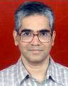
Mahesh B. Patil

Mahesh B. Patil received B. Tech. from IIT Bombay, M.S. from the University of Southern California and PhD from the University of Illinois at Urbana-Champaign, all in Electrical Engineering. His current areas of interest are circuit simulation, and applications of stochastic optimisation.

Qualifications

• B. Tech (EE), IIT Bombay, 1984 M.S. (EE), University of Southern California, 1987 Ph.D. (EE), University of Illinois at Urbana-Champaign, 1992

Research Interests

• Circuit simulation
• Semiconductor device modelling and simulation
• Real-time simulation of power electronic circuits and systems
Simulation Tools

Work Experience

• University of Illinois: as a graduate student, worked on fabrication of HEMT’s and Monte Carlo simulation of compound semiconductor devices (1987-1992). Central Research Laboratory, Hitachi, Tokyo: as a Visiting Researcher, worked on simulation of MOS transistors

Journal Papers


  1. Mahesh Patil, Ruchita Korgaonkar, and Kumar Appaiah, "GSEIM: a general-purpose simulator with explicit and implicit methods", Sadhana, vol. 46, pp. 206, Oct. 2021. [DOI]
  2. M B Patil, U Ramakrishna, and S C Mohan, "Multi-objective optimisation of damper placement for improved seismic response in dynamically similar adjacent buildings", Sadhana, vol. 45, Aug. 2020. [DOI]
  3. Mahesh B Patil, "Improved performance in multi-objective optimization using external archive", Sadhana, vol. 45, Mar. 2020. [DOI]
  4. Mahesh Patil, M. Naveen Naidu, A. Vasan, and Murari R. R. Varma, "Water Distribution System Design Using Multi-Objective Particle Swarm Optimisation", Sadhana, vol. 45, no. 21, Jan. 2020. [DOI]
  5. S. Roymohapatra, G. R. Gore, A. Yadav, M. B. Patil, K. S. Rengarajan, S. S. Iyer, and M. Shojaei Baghini, "A Novel Hierarchical Circuit LUT Model for SOI Technology for Rapid Prototyping", IEEE Transactions on Computer-Aided Design of Integrated Circuits and Systems, pp. 1-1, 2019. [DOI]
  6. A. Chopde, D. Magare, M. Patil, R. Gupta, O.S. Sastry, "Parameter Extraction for Dynamic PV Thermal Model Using Particle Swarm Optimization", Applied Thermal Engineering, vol. 100, pp. 508-517, 2016.
  7. R. A. Thakker, M. Srivastava, K. H. Tailor, M. Shojaei Baghini, D. K. Sharma, V. Ramgopal Rao, and M. B. Patil , "A Novel Architecture for Improving Slew Rate in FinFET-based Op-Amps and OTAs", Elsevier Microelectronics Journal, vol. 42, pp. 758–765, May 2011.
  8. R. A. Thakker, C. Sathe, M. Shojaei Baghini, and M. B. Patil, "A Table-Based Approach to Study the Impact of Process Variations on FinFET Circuit Performance", IEEE Transactions on Computer-aided Design of Integrated Circuits and Systems, vol. 29, no. 4, pp. 627-631, Apr. 2010.
  9. R. A. Thakker, M. Shojaei Baghini, and M. B. Patil, "Automatic Design of Low-Power Low-Voltage Analog Circuits using PSO with Re-initialization", Journal of Low-Power Electronics, vol. 5, no. 3, pp. 291-302(12), Oct. 2009.
  10. B.P.Harish, N.Bhat, and M.B.Patil,, "On a generalized framework for modeling the effects of process variations on circuit delay performance using response surface methodology", IEEE Trans CAD of ICs and Systems, vol. 26, no. 3, pp. 606-614, Mar. 2007.
  11. B.P.Harish, N.Bhat, and M.B.Patil, "Analytical modeling of CMOS circuit delay distribution due to concurrent variations in multile processes", Solid-State Electron, vol. 50, no. 7-8, pp. 1252-1260, Aug. 2006.
  12. D.Vinay Kumar, K.Narasimhulu, M.Shojaei Baghini, D.K.Sharma, M.B.Patil, and V. R.Rao, "Evaluation of the impact of layout on device and analog circuit performance with LAC MOSFETs", IEEE Trans. Electron Devices , vol. 52, no. 7, pp. 1603-1609, Jul. 2005.
  13. S.N. Agarwal, A.Jha, D.Vinay Kumar, J.Vasi, M.B.Patil, and S.C.Rustagi, "Look-up table approach for RF circuit simulation using a novel measurement technique", IEEE Trans. Electron Devices , vol. 52, no. 5, pp. 973-979, May 2005.
  14. M.V.Rammohan Reddy, D.K.Sharma, M.B.Patil, and V.R.Rao, "Power area evaluation of various double gate RF mixer topologies", IEEE Electron Dev. Lett. , vol. 26, no. 9, pp. 664-666, 2005.
  15. A.S.Roy, J.Vasi, and M.B.Patil, "A new approach to model non quasi static effects for MOSFETs Part II Small signal analysis", IEEE Trans. Electron Devices , vol. 50, no. 12, pp. 2401-2407, Dec. 2003.
  16. A. S.Roy, J. Vasi, and M.B.Patil, "A new approach to model non quasi static effects for MOSFETs Part I Large signal analysis", IEEE Trans. Electron Devices , vol. 50, no. 12, pp. 2993-2400, Dec. 2003.
  17. M.B.Patil, M.C.Chandorkar, B.G.Fernandes, and K.Chatterjee, "Computation of steady-state response in power electronic circuits", IETE J. Research , vol. 48, no. 6, pp. 471-477, Nov. 2002.
  18. M.B. Patil, "A public domain program for mixed signal simulation", EEE Trans. Education, pp. 187-193, May 2002.
  19. B.J.Daniel, C.D.Parikh, and M.B.Patil, "Modelling of the CoolMOS transistor Part I: Device physics", IEEE Trans. Electron Devices , pp. 916-922, May 2002.
  20. M.B.Patil, S.P.Das, A.Joshi, and M.C.Chandorkar, "A new public-domain simulator for power electronics circuits", IEEE Trans. Education , vol. 45, no. 1, pp. 79-85, Feb. 2002.
  21. P.Ravi Kumar, P.Sharma, and M.B.Patil, "Validation of small-signal model of a forward-biased p-n junction diode,", Solid-St. Electron, vol. 44, pp. 1247-1253, 2002.
  22. M.B.Patil, "Extension of the VR discretization scheme for velocity saturation", IEEE Trans. CAD, vol. 18, pp. 1508-1511, 1999.
  23. M.B.Patil, "New discretization scheme for two-dimensional semiconductor device simulation on triangular grid", IEEE Trans. CAD, vol. 17, pp. 1160-1165, 1998.
  24. M.B. Patil, "New approach for two-dimensional semiconductor device simulation on curvilinear grids", Solid-St. Electron, vol. 41, pp. 789-792, 1997.
  25. U.Ravaioli, C.Lee, and M.B.Patil,, "Monte Carlo simulation of microwave devices", Math. Comput. Modelling, vol. 23, no. 8, pp. 167-169, 1996.
  26. M.B.Patil, Y.Ohkura, T.Toyabe, and S.Ihara, "On coupling the drift-diffusion and Monte Carlo models for MOSFET simulation", Solid-St. Electron, vol. 38, no. 4, pp. 935-936, 1995.
  27. M.B.Patil, Y.Okuyama, Y.Ohkura, T.Toyabe, and S.Ihara, "Transmission matrix approach for electron transport in inversion layers", Solid-St. Electron, vol. 37, no. 7, pp. 1359-1365, 1994.
  28. M.B.Patil, U.Ravaioli, and M.Hueschen, "Monte Carlo Simulation of Real-Space Transfer Transistors Device Physics and Scaling Effects", IEEE Trans. Electron Devices, vol. 40, no. 3, pp. 480-486, 1993.
  29. M.B.Patil, U.Ravaioli, and K.Hess, "Real-Space Transfer in AlGaAs-GaAs Heterojunctions in Properties of AlGaAs", EMIS Datareview Series, pp. 214-220, Feb. 1992.
  30. M.B.Patil and U.Ravaioli, "Monte Carlo analysis of real-space transfer in a three-terminal device", J. Appl. Phys, vol. 72, no. 1, pp. 161-167, 1992.
  31. M.B.Patil and U.Ravaioli, "Transient simulation of semiconductor devices using the Monte Carlo method", Solid-St. Electron, vol. 34, no. 10, pp. 1029-1034, 1991.
  32. S. Noor Mohammad, M.B.Patil, J.J.Chen, M. S. Unlu, and H.Morkoc, "Analytical model for I-V characteristics of JFETs with heavily doped channels", Solid St. Electron, vol. 33, no. 1, pp. 53-64, 1990.
  33. M.B. Patil and U. Ravaioli , "Analytical approximation for wave functions and computation of scattering rates in double heterojunction structures", Superlattices and Microstructures , vol. 8, no. 4, pp. 459-466, 1990.
  34. M. B. Patil and U.Ravaioli, "Calculation of electron density in planar-doped high electron mobility transistors", Solid St. Electron., vol. 33, no. 7, pp. 953-962, 1990.
  35. M. B. Patil and H. Morkoc, "Self-consistent calculation of electron density in a two-channel modulation-doped field-effect transistor", Solid-St. Electron, vol. 33, no. 1, pp. 99-104, 1990.
  36. M. B. Patil, S. N. Mohammad, and H. Morkoc , "Modeling of field-effect transistors with laterally graded doping", Solid-St. Electron, vol. 32, no. 9, pp. 791-795, 1989.
  37. D. S. L. Mui, M. B. Patil, and H. Morkoc, "Calculation of the electron wave function in a graded-channel double-heterojunction modulation-doped field-effect transistor", Appl. Phys. Lett, vol. 55, no. 12, pp. 1223-1225, 1989.
  38. D. Mui, M. Patil, J.Chen, S. Agarwala, N.S. Kumar and H.Morkoc,, "Modeling of the I-V characteristics of single and double barrier tunneling diodes using a k.p band model", Solid-St. Electron, vol. 32, no. 11, pp. 1051-1031, 1989.
  39. S. Agarwala, M. B. Patil, C. K. Peng, and H. Morkoc, "AlGaAs/GaAs metal-insulator-semiconductor-type field-effect transistor fabricated on InP substrate", Appl. Phys. Lett, vol. 53, no. 6, pp. 493-494, 1988.
  40. M. B. Patil, S. Agarwala, and H. Morkoc, "Back-gated field-effect in a double heterostructure modulation-doped field-effect transistor", Electron. Lett, vol. 24, no. 15, pp. 925-926, 1988.
  41. M. B. Patil, D. Mui, S. Kalem, and H. Morkoc, "Reduced backgating effect in modulation-doped field-effect transistors by p-n junction isolation", Appl. Phys. Lett, vol. 53, no. 24, pp. 2417-2419, 1988.
  42. J. H. Shieh, M. B. Patil, and B. J. Sheu, "Measurement and analysis of charge injection in MOS analog switches", IEEE Trans. Solid-State Circuits vol., vol. SC-22, no. 2, pp. 277-281, 1987.
Conference Papers / Book Chapters

  1. Akhil Nandan and Mahesh Patil, "Comparison of GSEIM with Simulink with respect to simulation speed" in 2022 IEEE International Conference on Signal Processing, Informatics, Communication, and Energy Systems, May 2022.
  2. Sandeep Nair and Mahesh Patil, "Woodbury Matrix Update Method for Inverse Admittance Matrix Formulation in Real-Time Simulation of Power Electronic Circuits" in Published in: 2018 IEEE International Conference on Power Electronics, Drives and Energy Systems (PEDES) , IEEE, Dec. 2018.
  3. S. Roymohapatra, G. R Gore, A. Yadav, M. B. Patil, K. S Rengarajan, and M. Shojaei Baghini, "Enhanced Look-up Table Approach for Modeling of Floating Body SOI MOSFET" in IEEE iNIS, India, Dec. 2017.
  4. Sitansusekhar Roymohapatra, Ganesh R Gore, Akanksha Yadav, Mahesh B. Patil, Krishnan S Rengrajan, Maryam Shojaei Baghini, "Enhanced Look-Up Table Approach for Modeling of Floating Body SOI MOSFET" in IEEE-iNIS 2017, IEEE, pp.6, Dec. 2017.
  5. A. Chopde, D. Magare, M. Patil, R. Gupta, O.S. Sastry, "Accurate Prediction of Electric Power for Photovoltaic Modules using Particle Swarm Optimzation" in IEEE PVSC, Dec. 2016.
  6. C. S. Solaki, B. G. Fernandes, B. M. Arora, P. Sharma, V. Agarwal, M. B. Patil, J. Vasi, D. B. Phatak, M. Atrey, K. Moudgalya and K. Bijlani, "Teach a 1000 Teachers: A methodology for the rapid ramp-up of photovoltaics manpower required for India’s national solar mission" in 38th IEEE Photovoltaic Specialists Conference, Austin, USA, Dec. 2012.
  7. S. Prajapati, R.A.Thakker, M. Shojaei Baghini, and M.B.Patil, "Performance Evaluation of FinFET and Planar MOSFET Devices at Circuit Level for 45nm Technology" in IEEE/VSI VDAT Symposium, India, Jul. 2010.
  8. A. B. Sachid, R. A. Thakker, C. Sathe, M. Shojaei Baghini, D. K. Sharma, V. R. Rao, and M. B. Patil, "Auto-BET-AMS: An Automated Device and Circuit Optimization Platform to Benchmark Emerging Technologies for Performance and Variability using an Analog and Mixed-Signal Design Framework" in IEEE ISQED, USA, pp.713 - 720 , Mar. 2010.
  9. R. R. Navan, R. A. Thakker, S. P. Tiwari, M. Shojaei Baghini, M. B. Patil, S. G. Mhaisalkar, and V. R. Rao, "DC & Transient Circuit Simulation Methodologies for Organic Electronics" in IEEE IEDST, India, Jun. 2009.
  10. R. A. Thakker, M. Shojaei Baghini, and M. B. Patil, "Low-Power Low-Voltage Analog Circuit Design using HPSO" in IEEE Int. Conf. on VLSI Design, India, (Sister Conf. of IEEE DAC, DATE and ICCAD), pp.427-432, Jan. 2009.
  11. R. R. Navan, R. A. Thakker, S. P. Tiwari, M. Shojaei Baghini, M. B. Patil, S. G. Mhaisalkar , and V. Ramgopal Rao, , "DC and transient circuit simulation Methodologies for organic electronics", Proc. second Int. Workshop on Electron Devices and Semiconductors, 2009.
  12. R. A. Thakker, C. Sathe, A. B. Sachid, M. Shojaei Baghini, V. R. Rao, and M. B. Patil, "Automated Design and Optimization of Circuits in Emerging Technologies" in IEEE ASP-DAC, Japan, (Sister Conf. of IEEE DAC , DATE and ICCAD), pp.504 - 509 , Jan. 2009.
  13. A. B. Sachid, M. Shrivastava, R. A. Thakker, M. Shojaei Baghini, D. K. Sharma, M.B.Patil, and V. R. Rao , "Technology-Aware Design (TAD) for Sub-45nm CMOS Technologies" in Intel Corporation AAF, Taiwan, (Received the best research paper award in circuit design category), Nov. 2008.
  14. R. A. Thakker, C. Sathe, A. B. Sachid, M. S. Baghini, V. R. Rao , and M. B. Patil, "Automated Design and Optimization of Circuits in Emerging Technologies", IEEE ASP-DAC , 2009.
  15. R. A. Thakker, M. B. Patil, and K. G. Anil, "Parameter extraction for Advanced MOSFET model using particle swarm optimization", Workshop on Compact Modeling NanoTech-2008, 2008.
  16. A. B. Sachid, M. Srivastava, R. A. Thakker, M. Shojaei Baghini, D. K. Sharma, M.B.Patil, and V. Ramgopal Rao, "Technology-Aware Design (TAD) for Sub-45nm CMOS Technologies", Intel Asia Academic Forum , 2008.
  17. R.A.Thakker and M.B.Patil, "Hierarchical particle swarm optimization with genetic operations and intensive local search", Int. Conf. Advances in Control and Optimization of Dynamical Systems (ACODS-2007), 2007.
  18. B.P.Harish, N.Bhat, and M.B.Patil, "Process variability-aware statistical hybrid modeling of dynamic power dissipation in 65 nm CMOS designs", Int. Conf. Computing: Theory and Applications, 2007.
  19. P. Jain, D. V. Kumar, J. Vasi and M. B. Patil, "Evaluation of non-quasi-static effects during SEU in deep submicron MOS devices and circuits" in Proceedings of the 19th International Conference on VLSI Design (VLSI’06), Dec. 2006.
  20. A. M. Chopde, S. Khandelwal, R. A. Thakker, M. B. Patil, and Anil K. G., "Parameter extraction for MOS model 11 using particle swarm optimization", International Workshop on Physics of Semiconductor Devices, 2007.
  21. B.P.Harish, M.B.Patil, and N.Bhat, "Modeling of the effects of process variations on circuit delay at 65 nm", Proc. IEEE Int. Conf. Electron Devices and Solid-State Circuits, 2005.
  22. A. Jha, J. Vasi, S. C. Rustagi and M. B. Patil, "A novel method to obtain 3-port network parameters for a MOSFET from 2-port measurements" in International Conference on Microelectronic Test Structures, Hyogo, Japan, Dec. 2004.
  23. A.Jha, J.Vasi, S.C.Rustagi, and M.B.Patil, "A novel method to obtain 3-port network parameters from 2-port measurements", Proc. IEEE Int. Conf. Microelectronic Test Structures, 2004.
  24. Dennis Sasikumar, R.Manchanda, and M.B.Patil, "The role of dendritic spines in EPSP amplification: a computational pilot study using a novel simulation platform", Int. Symp. Neuroscience, Dec. 2003.
  25. D.Vinay Kumar, N.Mohapatra, M.B.Patil , and V.R.Rao, "Application of look-up table approach to high-K gate dielectric MOS transistor circuits", Proc. VLSI Design, Jan. 2003.
  26. P.N.Kondekar, C.D.Parikh, and M.B.Patil,, "Analysis of breakdown voltage and on resistance of super-junction power MOSFET using theory of novel voltage sustaining layer", Proc. 33rd IEEE Power Electronics Specialist Conference, Jun. 2002.
  27. M.B.Patil, "A new mixed-signal simulator", Proceedings of the National Seminar on VLSI Systems, Design, and Technology, Dec. 2002.
  28. D.Vinay Kumar, R.A.Thakker, M.B.Patil, and V.R.Rao, "Simulation study of non quasi static behaviour of MOS transistors", Proc. 5th International Conference on Modeling and Simulation of Microsystems, Apr. 2002.
  29. D. R. Nair, M. B. Patil and J. Vasi, "Extraction of effective mass of carriers in Si3N4 by accurate modeling of gate tunneling current" in 32nd IEEE Semiconductor Interface Specialists Conference (SISC 2001), Washington, DC , Dec. 2001.
  30. Deleep R.Nair, M.B.Patil, and J.Vasi, "Extraction of Effective Mass of Carriers in Si 3N 4 by Accurate Modeling of Gate Tunneling Current", 32nd IEEE Semiconductor Interface Specialists Conference, Dec. 2001.
  31. M.B.Patil, U.Ravaioli, and T.Kerkhoven, "Numerical comparison of some iterative schemes for semiconductor device simulation", Fifth International Workshop on Computational Electronics, May 1997.
  32. M.B.Patil, U.Ravaioli, K.Hess, and M.Hueschen, "Monte Carlo simulation of InGaAs AlGaAs GaAs real space transfer transistors", Seventh International Conference on Hot Carriers in Semiconductors, Jul. 1991.
  33. M.B.Patil and U.Ravaioli, "A novel real space transfer transistor Monte Carlo simulation results", International Semiconductor Device Research Symposium, Dec. 1991.
Patents

  1. Sandeep Nair and Mahesh Patil,"A matrix update method for admittance matrix formation in real-time simulation of power electronic circuits", India Patent (NA) issued in April 2017 .
  2. R. A. Thakker, M. Shrivastava, M. Shojaei Baghini, D. K. Sharma, Ramgopal V. Rao, and M. B. Patil,"Operational Amplifier Having Improved Slew Rate", Patent filed in March 2010 (India), USA Patent (US Patent (8089314)) issued in January 2012 .
Miscellaneous

  1. M. B. Patil, "Circuit simulation using explicit methods: singular matrix issues." arXiv preprint available at [https://arxiv.org/abs/2306.13489] (2023).
  2. M. B. Patil and V.V.S. Pavan Kumar Hari, "Circuit simulation using explicit methods," available at [https://arxiv.org/abs/2301.04595] (2023).

Address

IIT Bombay was established in the year 1957 and the department of Electrical Engineering (EE) has been one of its major departments since its inception.

Contact Us

IIT Bombay was established in the year 1957 and the department of Electrical Engineering (EE) has been one of its major departments since its inception.

Contact Us

IIT Bombay was established in the year 1957 and the department of Electrical Engineering (EE) has been one of its major departments since its inception.

Contact Us

About | IITBEducation | Research | Site Map | Feedback | RTI | Contact Us

© 2023, IITB. All rights reserved.

About | IITBEducation | Research | Site Map | Feedback | RTI | Contact Us

© , IITB. All rights reserved.

About | IITBEducation | Research | Site Map | Feedback | RTI | Contact Us

© 2023, IITB. All rights reserved.